


One of the joys of working with basic digital electronics– and logic gate ICs in particular –is that it almost works like building with a set of Lego blocks: One output goes here, which connects to the next input here, and so forth until it does what you wanted.
If you’ve played with chips like these, you’ve probably also come across chips with “open collector” outputs. And if not, they’re worth knowing about. Open-collector outputs form the basis of a number of clever tricks for level-shifting and interfacing between different types of logic, and from logic to other types of electronic circuits.
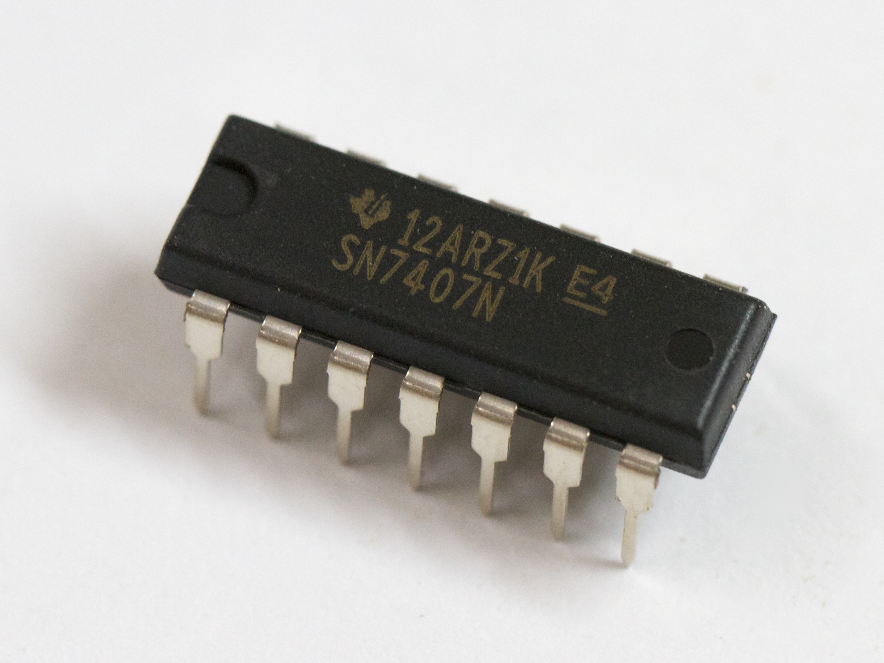
In what follows, we’ll work with the SN7407N, which is one of the most basic ICs with open-collector outputs. We’ll discuss what it means to have “open collector” outputs, and show some of the different ways that they are used.
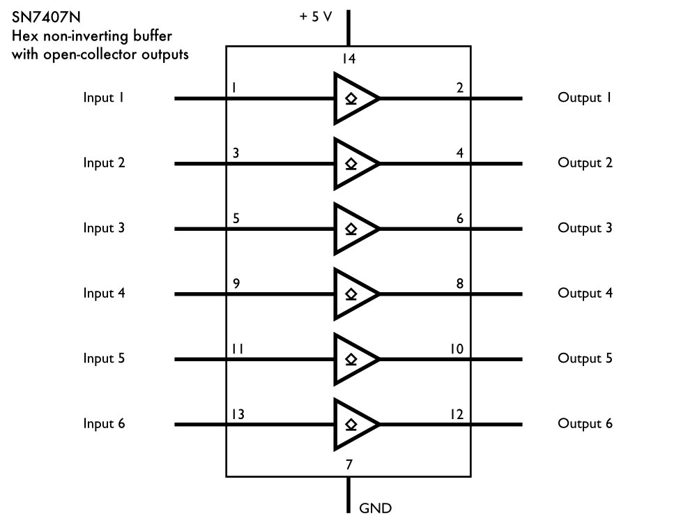
This is a schematic symbol for the SN7407N, showing the pinout. There’s power (nominal 5 V) and ground, and then six input-output pairs, for a total of 14 pins.
The chip is described as a hex buffer (or hex driver), because there are six independent channels, and the logic function is that each output gives a continuous copy of its input.
The logic function of “buffer” is normally indicated on a schematic symbol by the forward-triangle “amplifier” symbol on each channel– a buffer is just an amplifier with “unity” (X1) gain –and the symbol is modified by the underlined diamond mark that indicates open collector outputs.
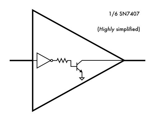
Here’s a simplified model of what is inside each buffer channel.
The buffer input goes into a logical NOT gate. The output of that NOT gate goes to the base of an NPN bipolar transistor. The emitter of the transistor is connected to ground and the collector of the transistor is connected to the output. This is the “open collector.”
When a logical input to the SN7407N is low, the output of the NOT gate is high, so the base of the transistor is held at a voltage above the emitter. This “turns on” the transistor, which means that if there is any voltage (above about 1.5 V) connected to the collector– that is, connected to the output of the SN7407N channel –current will flow from the collector, through the transistor to ground.
When a logical input to the SN7407N is high, the output of the NOT gate is low, so the base of the transistor is held low, at the same voltage as the emitter. The transistor is off, and does not conduct current. That is to say, no current flows to or from the output. It’s as though the output is simply not connected to anything.
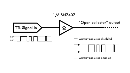
So, where with most digital electronics, the output of a buffer (or other logic gate) is a “high” or “low” voltage, an open collector has two different states: Output transistor disabled or output transistor enabled. In other words, output (effectively) “not connected” or output connected, through a transistor, to ground.
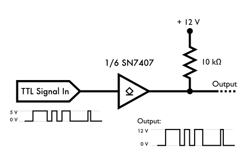
Here is a most basic example of how that can be useful. Suppose that an open collector output is outfitted with a “pull-up ” resistor– a moderate value resistor (typically 2.2k – 10k) connected to a positive power supply rail, say 12 V.
Then, when the output transistor is disabled (and the output is effectively “not connected”), the output will be pulled up to the power supply rail value, 12 V in this case. When the output transistor is enabled, the output is effectively connected to ground, and the output goes close to 0 V.
This, therefore, is a neat way to build a logic-level shifter. What we’ve done is translate a logic-level input (e.g., 0-5V) into a different level (0-12 V). Note that the output does not have to be pulled up that far. If the pull-up were connected to 3V, the output range would be 0-3 V, and you could use that as an input to digital electronics that do not tolerate a full 5 V on their inputs. For the SN7407N, the output can go as high as 30 V, so you can also use it to shift higher as well.
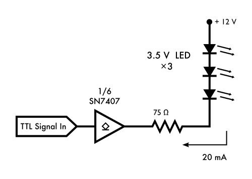
Another way that you can use open collector outputs is as a compact substitute for a set of external, discrete transistors. Suppose that you wanted to drive six sets of three white LEDs each, controlled by six outputs from your microcontroller. To do this, you might hook up each output, through a resistor, to the base of a transistor, and use that transistor to switch the current to the LEDs. The SN7407N could be used the same way– allowing you to substituting one chip for six resistors plus six transistors.
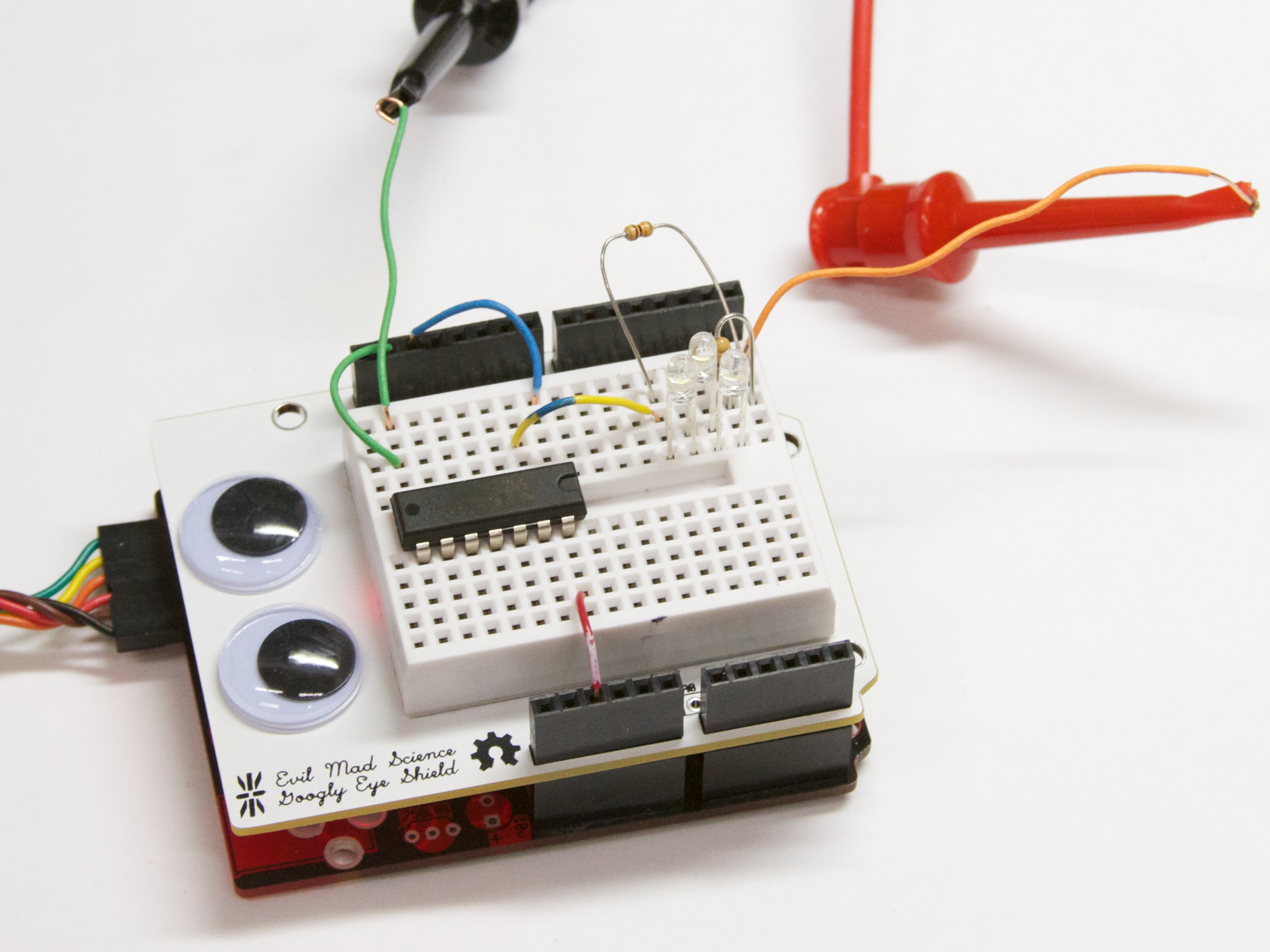
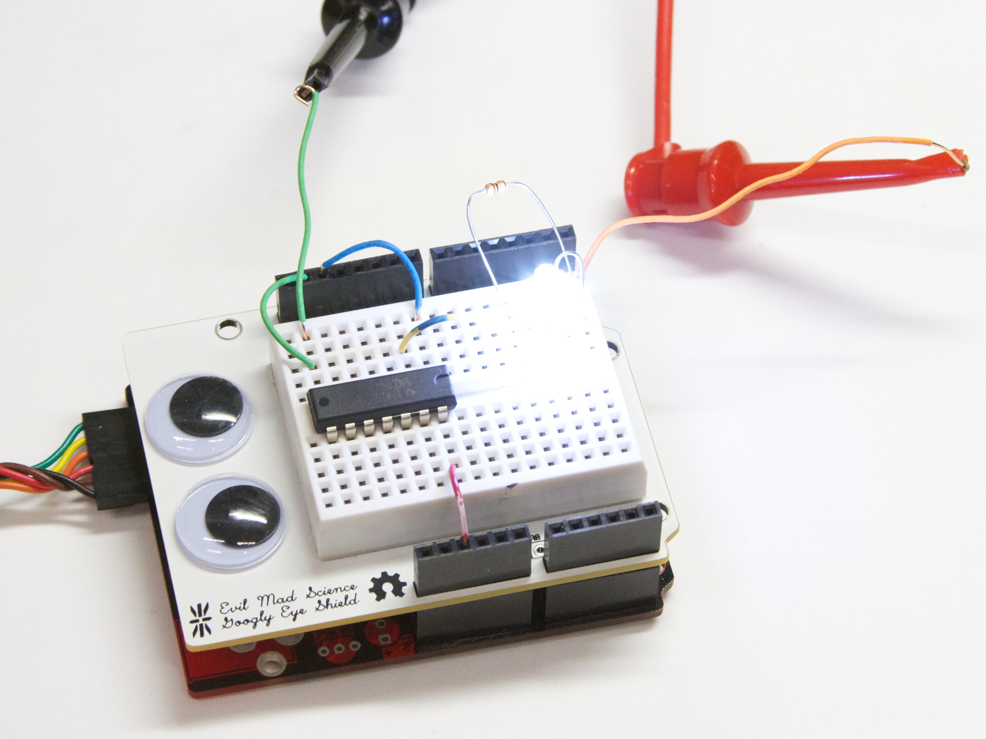
Here’s one channel of the last circuit, built on a breadboard. The blinking TTL input comes from the microcontroller, into the SN7407, and the external clip leads bring the 12 V on board. If you look closely, you’ll see that there’s actually one more component: a vestigial (but harmless) 10k pull-up on the SN7407 output.
This circuit is an example of a “low side” driver, where the LEDs are switched on and off from their “low side,” the side closer to ground potential.
There are some things that you can’t do with open collector outputs.
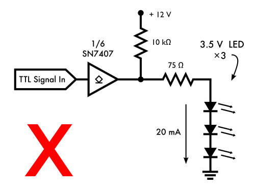
It’s tempting to think that because your output works to switch 20 mA, it can also be used to source 20 mA, as in the “bad circuit” above. It is true that in conjunction with a pull-up resistor, the open collector output can go up to 12 V, but that’s assuming that there is only minimalcurrent draw from that 12 V output. The issue is that the open-collector output does not source current at all; it only can sink current.
So, if any current were to flow through the LEDs, it would not come from the SN7407 output, but from the 12 V rail, through the 10k resistor. And by Ohm’s law, you can’t get 20 mA to pass through 10 k?, unless you provide at least 200 V. This circuit won’t come close.
The circuit above would be an example of a “high side” driver if it actually worked. High-side drivers switch LEDs (or other electronics) on and off, using a switch connected to the side at higher voltage. There’s actually a very real need for both “high side” and “low side” driver circuits. For example, in a multiplexed LED matrix, each row is switched on one at a time, using a high-side driver connected to each row. Then, low-side drivers connected to each column dictate which LEDs in that row are on and off at a given time.
So how might we go about building a high-side driver that works? Since the open collector output with a pull-up won’t source the current that we need, the obvious thing to go back to regular logic (which can source and sink current), and instead place a real switch– a transistor –on the high side of the LEDs.
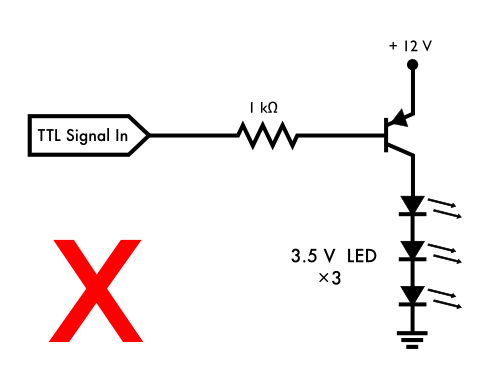
And so… we end up with another bad circuit. And as far as bad circuits go, this is one of the most common. The problem* is that in order to switch the LEDs on or off, the logic output needs to be able to swing the voltage of the transistor base both above and below the voltage at the top of the LED stack, very close to 12 V. As our logic input only ranges between 0 and 5 V, the LEDs will be always on (if a PNP transistor is chosen) or always off (if an NPN transistor is chosen).
*Aside: You may have noticed a second problem as well: Even if the transistor did turn on, this would still be a bad circuit because we forgot to put a resistor in series with the LEDs.
It turns out that we actually have an excellent case here for using one of those “level-shifting” circuits that we discussed earlier, so that we can raise the transistor inputs up to 12 V.
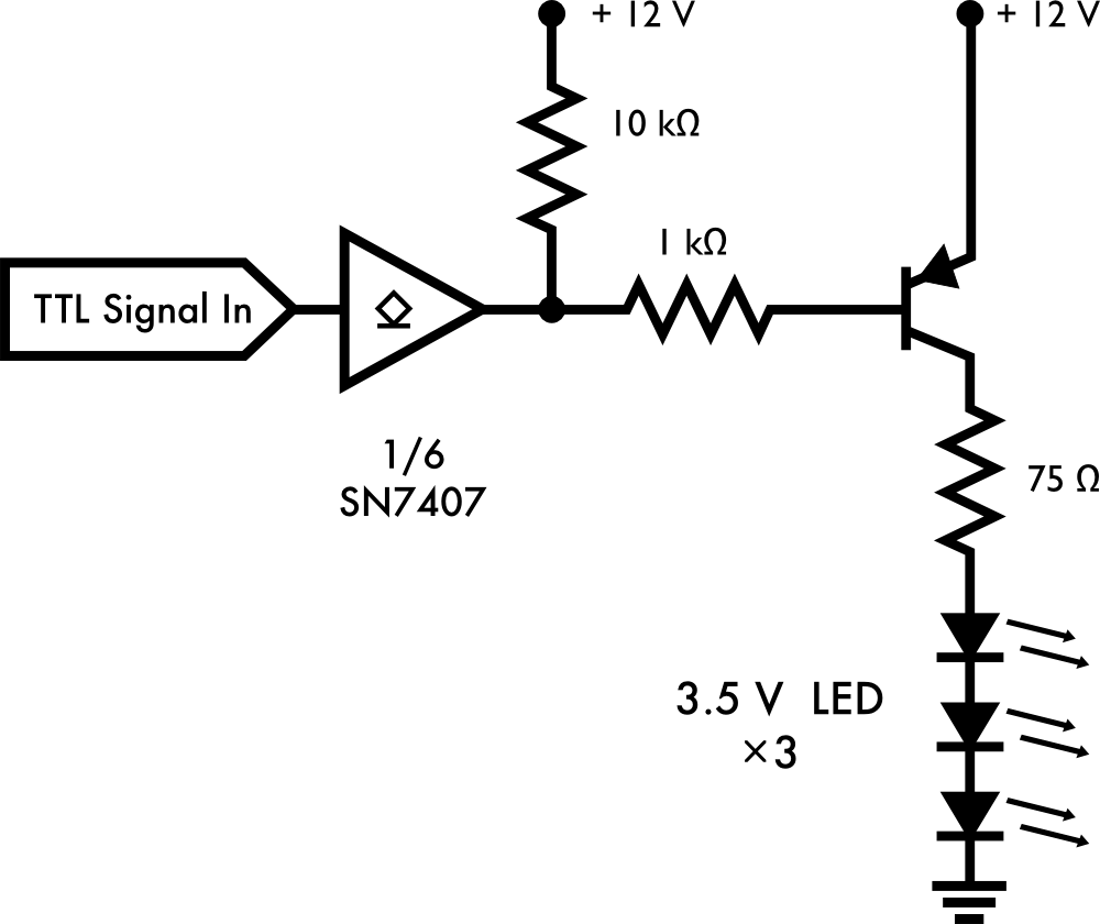
So here’s a solution that works, and it’s actually a great high-side driver.
The SN7407 output is pulled up to 12 V, through a 10 k? resistor. It is also connected, through 1 k?, to the base of a PNP transistor. When the SN7407 input is high, the outputs is effectively disconnected, and the base of the transistor is pulled up to 12 V, turning off the transistor, and ensuring that no current flows through the LEDs. When the SN7407 input is low, the base of the transistor is connected to ground through the 1 k? resistor, turning on the transistor, and thereby allowing the LEDs to turn on. So, a funny side effect of this is that this is not just a high-side driver, it’s an inverting high side driver– the LEDs are on when the input signal is low. If you wanted to reverse this, so that the LEDs were on when the input signal was high, you could simply replace the SN7407N with a SN7406N, the inverting equivalent of the SN7407N.
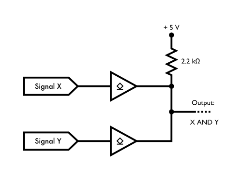
There’s yet another unique way that open collector outputs are useful, and that’s in building ad-hoc logic gates by connecting their outputs together.
Above is a simple example. Two SN7407 channels, from inputs X and Y have their outputs connected together and to a pull-up resistor. Then if both X and Y are high, the combined output will also be high. But, if either X or Y is low, the output will be low. This constitutes a logical AND gate, because the output is high if and only if both X and Yare high.
This kind of gate is referred to as a Wired-AND gate (because it’s made by wiring it up, rather than using a silicon AND-gate chip) and it’s a very useful type of gate. It’s particularly useful because you can connect dozensof open collector outputs to the same line, to make a very large AND gate that could (for example) monitor dozens of critical systems and trigger a shutdown if any of them fails.
Other types of wired logic gates can be built this way as well. For example, the above circuit built with inverting SN7406 channels would be a Wired-NOR gate that could be inverted again to yield a Wired-OR gate.
As a footnote, open collector “wired” logic gates like these have largely fallen out of favor. That’s partly because it’s hard to debug a hardware problem when you have dozens of gates connected together, and partly because of the development (long ago) of tristated logic chips. But they are still, on occasion, the right solution to a problem.
Further reading:
- Open Collector @ wikipedia
- Wired Logic @ wikipedia
- SN7407 product page @ TI
In the first "[TTL Signal In>" diagram, shouldn’t the Output Transistor Enabled label be at the bottom (output pulled low), and Output Transistor Disabled be at the top (output floats)?
Yes! Thank you! Fixed!
Windell H. Oskay
drwho(at)evilmadscientist.com
http://www.evilmadscientist.com/
A very interesting and instructive article. I shall be buying a few of these to play with!
Thanks Windell.
Awesome! Someone asked me just last week what open colector was and why anyone would want to use it.
Can I assume that "open drain" is the same as "open collector"?
The datasheet for the DS1307 that I am using in a project ATM indicates a pin-7 output that could be set for 1Hz "Open drain". I assume that a circuit like your first LED circuit could be used to provide an LED that flashed once a second. The example circuit in the datasheet uses an external pull-up so if nothing else it appears that your last circuit would work. Is that how you might use an "open drain" output?
It looks like you still need a current-limiting resistor in the high-side drive circuit, don’t you?
Yes, you are correct, and the figure should be corrected. I normally put the current regulation on the *low* side of the LEDs, but I apparently neglected it here, when putting everything on the high side.
Windell H. Oskay
drwho(at)evilmadscientist.com
http://www.evilmadscientist.com/
Aargh… I read "octopus"…
Still, I suppose that would be a fun project too.
Around 15 years ago I made up a joke related to this article:
Did you hear that they are having a golf tournament to celebrate the anniversary of the discovery of bipolar wired-or logic busses. Know what they’re going to call it? The Collector Open. :-)
Somehow my post of the wired-or joke got listed as "anonymous". It was posted by BillyBuggy, aka Bill Nye (not the…).
A particular example of the awesomeness of wired-AND gates is I2C busses. You can actually put signal X and signal Y at opposite ends of a wire, and read it off of each end, and the two ends of the wire can communicate with each other without the wire having an input end and an output end. If you’ve got a protocol with a clock line and a data line, you can have a bunch of devices on the same pair of lines, and a device can just start talking and shut up if it sees an unexpected zero, and somebody’s message will go through on each cycle without needing a special bus master.
In the sixth from the end paragraph there is a HTML typo for the ohm symbol (Omega), it appears to be missing a semicolon.
Search for:
10 k&Omega
Thanks! Fixed!
Windell H. Oskay
drwho(at)evilmadscientist.com
http://www.evilmadscientist.com/
Does any one have links explaining what can happens if you exceed VCC voltage on the input on such devices?
ie VIH > VCC?
Thanks