Category Archives: Electronics

Open Circuits: Now available

Earlier this year, I wrote about my then-forthcoming book, Open Circuits: The Inner Beauty of Electronic Components, co-written with our regular collaborator Eric Schlaepfer.

Open Circuits is a coffee table book full of close-up and cross-section photographs of everyday electronic components. And, it’s now shipping! As of today, it’s available in hardcover from your local bookstore, as well as to purchase online and in electronic versions.

Open Circuits, hardback

We also just launched a new website for the book, with links of where you can purchase it as well as lengthy galleries of images from the book and of outake photos.

We put up a list of sellers on the website, including direct from No Starch and our own store, where signed copies are available.

Flickery Halloween Fun

Shane from Dark Illusion Studios shared this video using our candle flicker LEDs to make skull sconces. Our flickering LEDs are great for lots of different Halloween projects.

If you still need some inspiration, check out our Halloween Project Archives:

Halloween is one of our favorite holidays, and … we’ve organized dozens of our Halloween projects into categories: costumespumpkinsdecor and food.

The 555SE and 741SE surface-mount soldering kits

555SE and 741SE kits

Today we are pleased to announce the release of two new soldering kits: the 555SE discrete 555 timer and the 741SE discrete op-amp.

Both of these new kits are surface mount soldering kits — our first surface mount soldering kits — and we think that you’re going to love them.

555 kits, big and small

You might be familiar with our Three Fives discrete 555 timer and XL741 discrete op-amp kits. Both are easy soldering kits that let you build working transistor-scale replicas of the classic 555 timer chip and the famous µA741 op-amp. Those two are constructed with traditional through-hole soldering techniques and are styled to like “DIP” packaged (through-hole) integrated circuits.

Our new 555SE and 741SE kits implement the same circuits, now with surface mount components, and are styled to look like smaller “SOIC” packaged (surface mount) integrated circuits, complete with a heavy-gauge aluminum leadframe stand. Side by side with their through-hole siblings, the new kits are exactly to scale, with half the lead pitch and a lower profile.

555SE kit for scale

The 555SE and 741SE kits each come with eight (tiny) color-coded thumbscrew binding posts that you can use to hook up wires and other connections.

You can also probe anywhere that you like in these circuits — something that you generally can’t do with the integrated circuit versions.

741SE kit close up

The new 555SE and 741SE circuit boards are black in color, with a gold finish and clear solder mask so that you can see the wiring traces between individual components. There are a few other neat details here and there, such as countersunk holes for mounting the board to the leadframe.

The surface mount components are relatively large, with 1206-sized resistors and SOT-23 sized transistors, and assembly is straightforward with our clear and comprehensive instructions. These kits are designed to be a joy to build, whether you’re an old hand at surface mount soldering, want some practice before tackling a project, or are introducing someone to it for the first time.

Family portrait

And here is the new family: XL741, the Three Fives, along with the new 741SE and 555SE.

You can find the datasheets and assembly instructions for these kits, as well as links to additional documentation, on their respective product pages.

Both new kits are part of our ongoing collaboration with Eric Schlaepfer, who we have worked with on a number of dis-integrated circuit projects including the four kits here and the MOnSter 6502.

MOnSter in a box

MOnSter 6502 in enclosure

For the past couple of years we have been working towards a public launch of the MOnSter 6502, our working transistor-scale replica of the famous MOS 6502 microprocessor.

One of the biggest pieces of the puzzle has been how to present it in such a way that shows off its beauty but also lets you see it in action. Here – finally – is the result of that effort: An elegant shadowbox frame with hidden electronics and integrated buttons.

If you’d like to see the MOnSter and its new prototype enclosure, this weekend is the perfect opportunity: we are exhibiting it at the 2019 Vintage Computer Festival West, August 3-4 at the Computer History Museum in Mountain View, California.

MOnSter 6502 in enclosure

Where to go from here? If everything goes well, we’ll be launching the MOnSter this fall. Stay tuned!

Uncovering the Silicon: μL914

At the 2018 Bay Area Maker Faire, our project Uncovering the Silicon showed off a number of simple and complex integrated circuits (with rather large feature size) under the microscope. We had a great time helping visitors look at the features and get a glimpse of what’s inside those black box integrated circuit packages. To take this to the next level for this year’s Maker Faire, we decided to try and close the loop; to take one simple integrated circuit and elucidate its workings well enough that visitors to our booth will be able to see every single component of the circuit, understand their function, and relate it to the macroscopic behavior of the chip. For this, we picked what turns out to be a rather obscure chip: the Fairchild μL914, which is a dual 2-input NOR gate. This chip belongs to the resistor–transistor logic (RTL) family.

uL914 IC closeup in circuit

Here’s what the chip looks like. It’s in a funny old “glob-top” can package with eight leads.

pinout

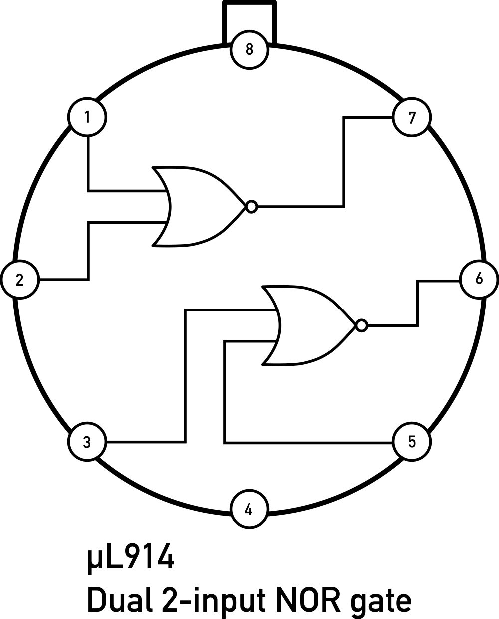
Here’s the pinout; there are two NOR gates in the chip, plus power and ground.

uL914 IC package circuit with switches and LEDs

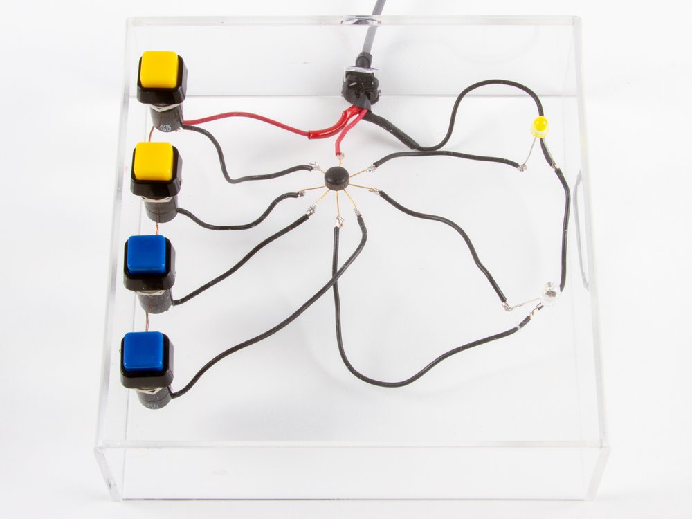
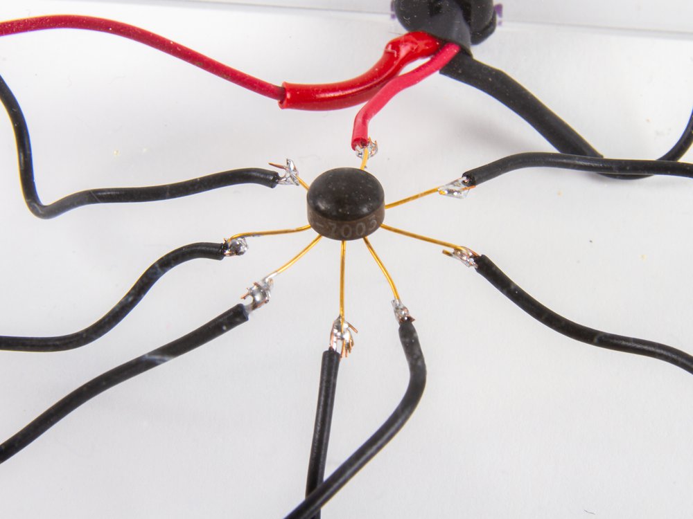
Ken Shirriff built a circuit with the chip to demonstrate its functionality. When we push either of the two buttons for one of the gates, that LED will turn off.

Schematic

Here’s the schematic diagram, adapted from the original datasheet. If you look at the left side, if either of those inputs goes high, the transistor pulls the output low.

uL914 dual 2-input NOR gate die photo

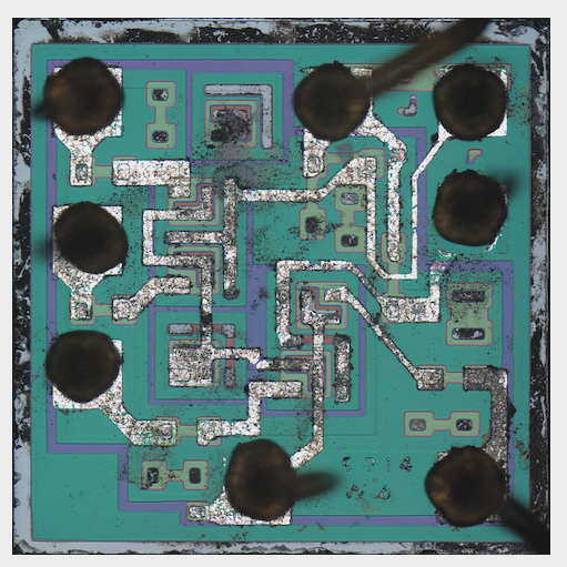
John McMaster decapped a few of the chips and sent us a die photo. He made a video about the process — no small feat. We’ll be bringing one of these bare chips and a microscope (equipped with both eyepieces and a camera) to Maker Faire.

For the macroscopic scale, we approached visualizing this circuit from a couple of angles: the physical structure of the chip, and the electronic structure of the circuit.

uL914 die model render

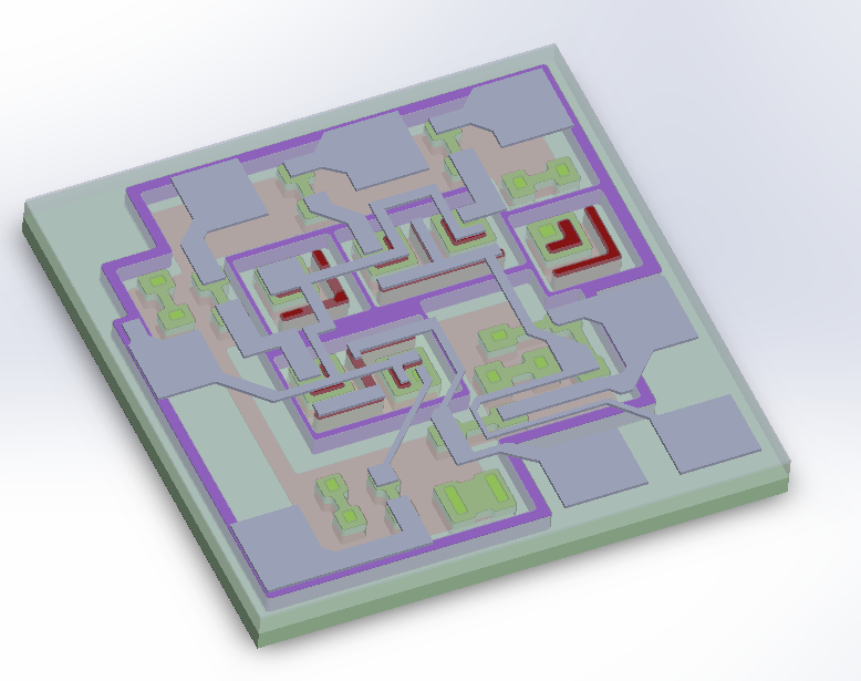
Eric Schlaepfer used the die photo to model the structure of the chip in CAD.

uL914 PCB version

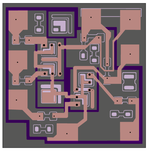
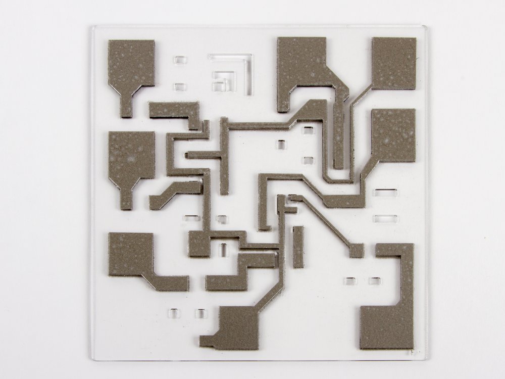
Simultaneously, Ken designed a printed circuit board version for use with discrete components that maintained the same structure as the IC.

Individual transistor acrylic model Individual transistor acrylic model

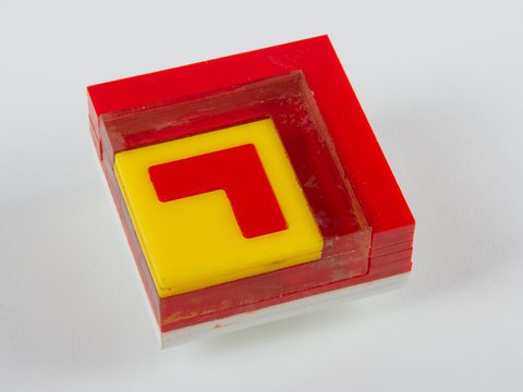
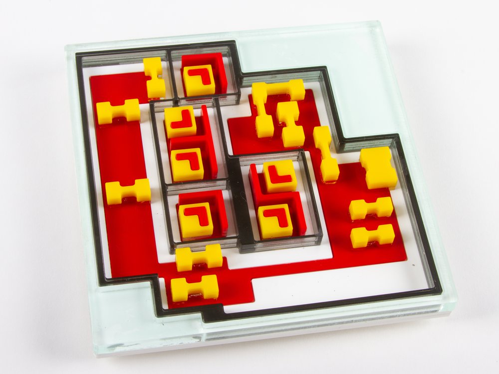
Working from Eric’s CAD model, we built a single NPN transistor model from layers of colored acrylic. If you lift it up, and look through the transparent middle layers, you can tell that the emitter (red) is embedded into the top of the base (yellow) and does not go all the down way through it. (Transistors like these are planar: The emitter is above the base, and the base is above the collector.)

The top layer of this little model has labels for the collector, emitter and base. It is removable so that the layers of the model can be more easily inspected.

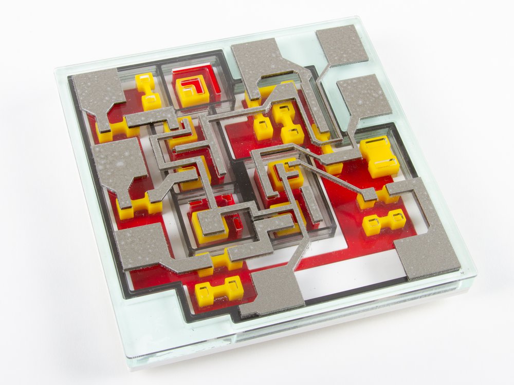
The model of the chip die includes a transparent cover representing the oxide layer, and that supports the metal layer with the wire bond pads on the edges.

One of the reasons that this particular chip is educational to look at is that there are a few unused components on the die. There are two unused transistors: one of them is unconnected, and the other is shorted. There are also several unused resistors (resistors are the dogbone shapes). The unconnected and unused components are easier to see, and provide a visual example that is useful for understanding what the connected components look like under the metal layer.

It is also fun to imagine what other circuits could have been made with different connections.

We glued most of the layers together, but left the top two layers removable so that it is easier to see the internal structure when the top is removed.

(Aside: we left out most of the epitaxial pocket material, because even though we used transparent acrylic to represent it, the layers of the components are much more visible without it present.)

Acrylic chip model top with metal layer

There are cutouts in the oxide layer where the metal layer connects to the circuitry below.

Acrylic chip model with hot glue bond wire example

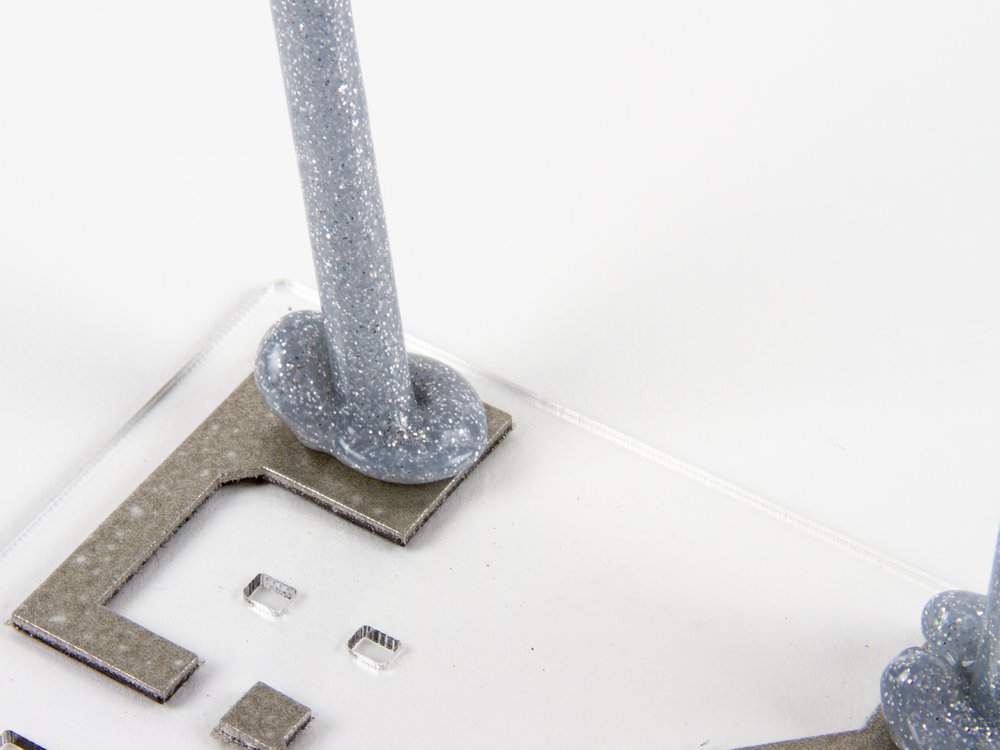
One of the most noticeable things you see when you look at this type of IC under the microscope is the bond wires. We’ve used silver glitter hot glue sticks to represent them.

bond wire closeup

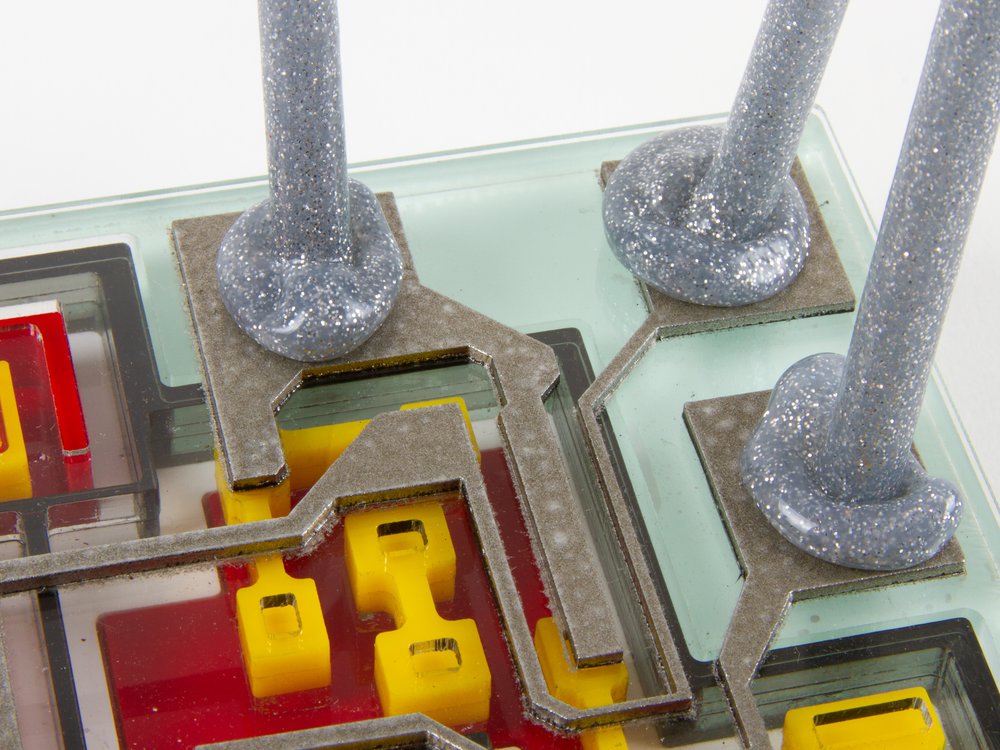
The glob of melted glue represents where the wire is bonded to the pad.

Acrylic chip model with hot glue bond wires

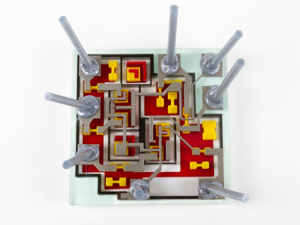
When you look straight down on the model with its glitter bond wires, it looks very similar to what you’ll see in the microscope.

Acrylic model legend

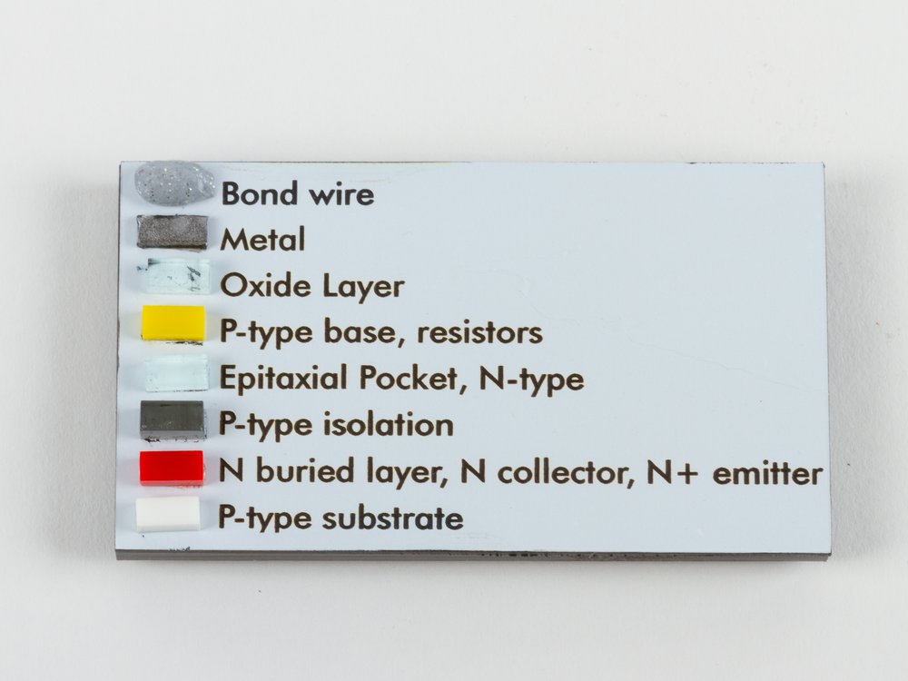
To round things out for our acrylic model, we made a physical legend to make it easier to identify all of the parts of the model.

uL914 discrete version switch and LED circuit

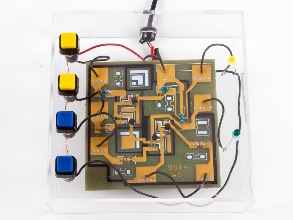
Once Ken got his PCBs back from our friends at OSHPark, he built it up with the same example circuit.

discrete circuit closeup

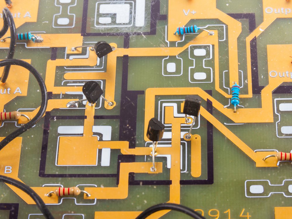
The PCBs turned out beautifully, and it’s great to see the familiar discrete packages on the enlarged circuit. Ken has published the PCB design on Github.

We hope to see you at Maker Faire this weekend!

Bonus: Ken laid out some hypothetical alternate metal layers to use the same die to create different chips.

Bonus video: Mike from Hackaday came to visit our project at Maker Faire and got a great video explanation of our project with Windell. He also wrote it up for Hackaday.