


In cooperation with Bunnie Studios, the blog of renowned hardware hacker Bunnie Huang (of Hacking the xbox and Chumby fame), we’re pleased to present an unusual “ware” that we acquired from one of our local Silicon Valley electronics surplus dealers.
(If you’re unfamiliar with the game, “Name that Ware” is a regular contest on Bunnie’s blog, where the goal is to learn about reverse engineering by analyzing unusual— or common but seldom-seen —hardware. You can read about the contest rules here, and you can see many pictures of past entries with this google image search, or even get a calendar featuring Name that Ware entries from prior years.)
In the detail photos that follow, we’ll show some close-up photos, and provide a little more physical description (without speculating too much as to the purpose of the different features). Can you identify this piece of hardware?

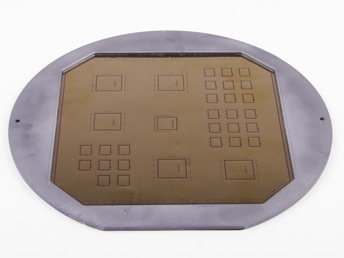
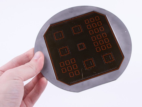
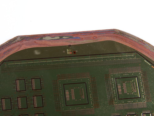
The outer edge of the object is a stainless steel frame, with a diameter of 150 mm with a flat indexing edge, giving it the basic shape of a “6 inch” IC wafer, by 2 mm in thickness.
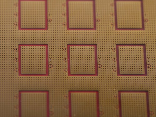
Stretched tight across the frame is a complex flex circuit, made of multiple layers of copper and Kapton film. The kapton film covers both side of the flex circuit almost entirely, giving it a variously brown or greenish sheen, depending on how the light catches it.
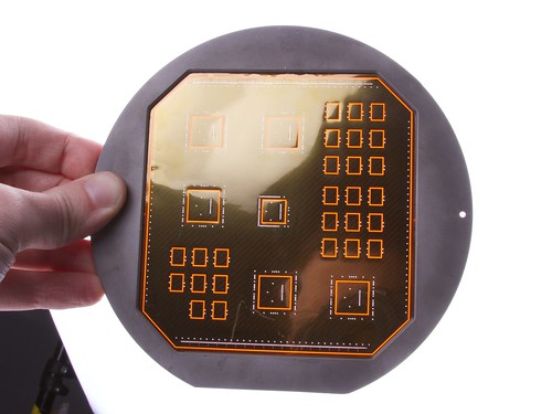
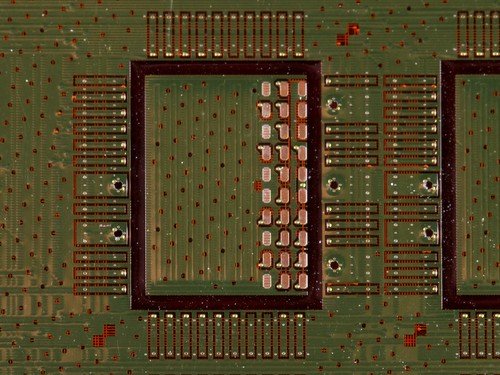
If you look through the ware at a light source, here are a few things that you might want to notice: (1) There are rectangular shapes that fully transmit light through the Kapton layers— indicating that these are electrically isolated areas (2) there is a similar octagonal isolation ring around the entire “wafer,” (3) there are tiny points of white light showing, indicating the presence of drilled through-holes or vias, and (4) there is a very weak diagonal pattern of diagonal stripes visible in the background of the circuitry.
Here are a few close-up views of those front-side features:
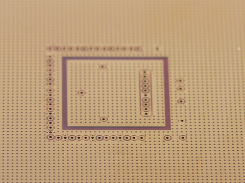

In the last picture, you may notice a little flash of silver around those through holes.
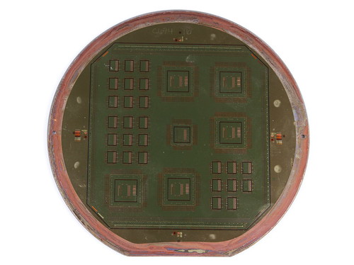
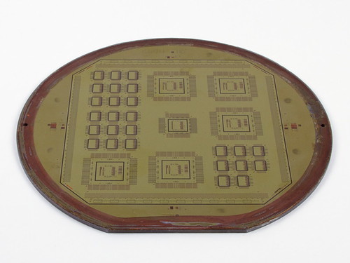
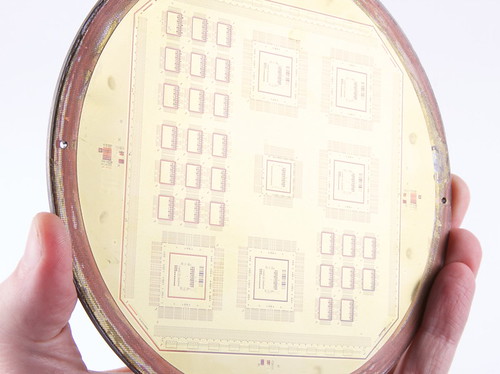
On the bottom side of the object, the flex circuit is bonded to the steel frame.
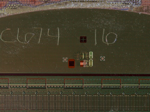
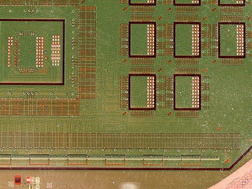
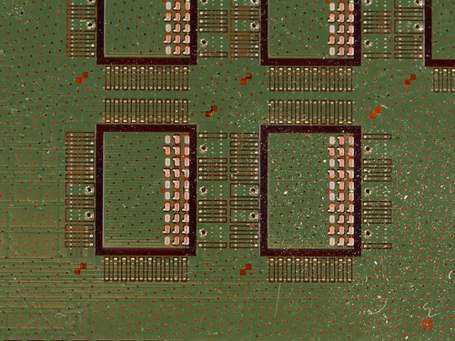
Some of these features resemble IC footprints, but you may also see that what would be solder pads on footprint are irregular and (mostly) covered by the top layer of greenish insulation.

The silver-colored oval and rectangular features within the square isolation ring are actually exposed metal contacts or pads of some sort.
Something else to notice if you look closely: In the gaps of the top copper layer, you can see a grid of selectively placed horizontal and vertical copper wires on different layers of the flex circuit.
So, if you have an inkling what you’re looking at, please leave your educated guesses (and reasoning) in the comments, here, or over at Bunnie Studios!
Update: We have the answer!

I’ll take the first guess and say a shield for testing completed circuit boards. The “vias” are where the test pins go through, the rest of the copper is shielding.
I love it!! This has to be the best mystery yet! Where does he find these things? I have successfully guessed some mystery items in the past, but this one’s got me stumped. I’ll definitely be watching for the correct answer!
I’d make the obvious guess that it’s a military app since they have the money to do expensive one-offs. But function?
Thanks for a great head scratcher!
I would say that it’s die substracts which are encapsulated in the plastic packaging. The die is paste in the middle and connections are done with wire bonding between die pads and small contacts that we see near the rectangular shapes. The double squares in the corners are alignment patterns for the packaging. It’s hold on this frame because the manufacturing process uses the same tools that for IC lithography.
This looks like it might be an incomplete flexible printed circuit. The little perforations in the copper layers are probably to compensate for differences in the thermal expansion between the other materials. The exposed pads look like they might bind with corresponding pads on a flipped-over IC. That leaves the more traditional looking pads to be exposed in another process (or is that why the NtW is not in use?) then wire-bonded in an IC wire-bonding to leadframe-type method? I don’t even know if it’s possible to make an IC that has pads top and bottom without a secondary substrate.
Mighty be some antennae or other high frequency device. If you look closely to the last two pictures you see some traces running special patterns below the top layer.
At least in the second last picture show a possible contact of the hidden traces to the pads on the top layer.
But what’s strange that the criss cross copper wis seem to run also behind the traces. So no transmission, more delay lines?
My guess for the more or less regular pattern of holes might also indicate a high frequency usage. They are used to make sure to have good grounding. For high current usage that’s also used but this dies not seem to be the case here.
But no clue what’s the thing is.
This one has me stumped. My first thought is a missile control board but it also looks like it is sized similar to a raw old 20cm wafer itself which suggests something… but I’m not sure what.
The 8 chip section and pair of 9 chip grids is suggestive of two banks of memory with ECC and one without.
Given its form factor, and the fact there are long rows of contacts on the rear forming a rectangle almost as big as the PCB itself, I’m gonna have to go with some sort of imaging device – maybe for a huge telescope or similar.
I’m imagining a huge CCD / CMOS sensor sitting on it, and then the whole thing fits into either a camera or a telescope or similar…
h
I would guess semiconductor fabrication equipment. Possibly related to silicon crystal ingot growing process control? No idea why they would take a flex circuit and then put it in such a stiff frame…maybe to achieve minimum thickness for a tight area without the risk of cracking a normal PCB. If it’s not fab equipment then it’s definitely weird enough for aerospace.
I am going to guess that it is a mask for a PCB etching process, possibly a UV or other similar near visible light process. Either that or an illuminati mind control device.
I’m guessing that it is a substrate for a multi-chip module, probably something insanely expensive (military, or something from Big Blue perhaps?).
The integrated circuit dies gets bonded directly to the substrate, explaining the lack of exposed metal pads for the IC pins. Only a small bond area is needed.
The larger outlined areas are probably for core logic while the smaller outlines are for cache memory.
The reason for the wafer-like surround is that the substrate is produced using an ordinary integrated circuit production line, probably something using older technology than the dies themselves. This older production line would havwe capacity to spare due to being replaced by newer technology.
looking like a circuit board for a outside of house electricity usage meter. its a long shot I know.
My guess – sensor head for a military earth-imaging satellite. Incomplete. The substrate would have chips solder-bump mounted on the various rectangular pads, another layer of heat-conductive filler applied to produce a level surface, then a single entire-wafer optical sensor glued on top and wire bonded to the outermost pad rows along 4 sides of the substrate. Then the thing would be glued to the back of the imaging system (where you can see cut-off glue around the edges of this one), and the rear of the substrate immersed in some cooling fluid.
The two holes near the edge of the metal frame are alignment pin holes, not screw holes.
What I can’t see – where are the power and IO connections?
If that’s not correct, and the device is NOT a chip carrying substrate, then could it be a kind of RF emissions stealthing shield? Something intended to be placed over a complex PCB, and parasitically hash the field emissions of the board by picking up emitted signals from high field strength points and spreading them out to produce anti-phase radiation?
But I think that’s a bizarre idea. Why not just enclose the original whatever in a decent shielding box?
Ah… maybe it’s something like that, but for reverse engineering an unknown design board, via analysis of RF emissions from the chips and PCB? With this providing a mix of shielding and RF pickup points?
Last grasp – maybe it’s an equivalent of the cold war projects doing things like digging vast, mysterious patterns of trenches in the desert, to give the Russian surveillance satellite operators nervous breakdowns.
I’ve always wanted to do something like that – build some freaky inexplicable alien-tech object, ding it up a bit, and just leave it somewhere like it fell from the sky.
VAX 9000 ECL gate array MCM substrate
http://www.dtjcd.vmsresource.org.uk/pdfs/dtj_v02-04_1990.pdf
page 80, VAX 9000 HDSC
And… we have a winner! Follow-up post coming soon!
Any idea what the faint diagonal lines are?
Wow! That’s astonishing. So that’s how the interconnects were done.
Also what a great ‘history of computing’ resource library. Very glad to hear about this.