


 So you’ve got a microcontroller and you want to use it to control something analog. That’s a common task, and a number of good solutions exist, depending on exactly what you need to do.
Most microcontrollers do not include built-in digital-to-analog conversion (DAC) hardware, and external converters cost money. There is, however, a quick, easy, and cheap little trick of a solution that can be played by averaging a digital output.
This is a short tutorial on making useful (but crude) analog output signals with a low-cost microcontroller. The analog signals will be made by averaging a digital pulse width modulation (PWM) output from one of the counter/timer units in the microcontroller, and do not require any dedicated digital to analog conversion hardware. We will first introduce some aspects of the counter/timer and discuss how it can be used to generate the pulse width modulation signal. After that, we’ll implement the scheme on an AVR microcontroller and use it to make a simple and slow little function generator circuit.
Doing things the quick and dirty way
The “obvious” solution for making an analog output signal from a digital device is to use a dedicated digital to analog converter (DAC), often an independent chip that can be extremely accurate, have very high resolution, and can change value very quickly. But, those cost money, and sometimes you just want to do it the quick and dirty way instead. Again, our trick is to use a pulse-width modulation (PWM) digital output signal, and average it with a low-pass filter to create the analog output signal. In comparison to using a true DAC, this method generally produces a less accurate, less precise, and slower analog signal. On the bright side– and it is indeed bright– this method is easier and faster to implement and it costs almost nothing. It’s quick and dirty D to A, and it can often get the job done.
This technique is hardly new; it’s one of the standard tricks known by people who know microcontroller programming tricks. There’s even an Atmel Application note on using the PWM outputs as analog outputs. However, if you haven’t seen this before, are just getting started with microcontrollers, or find the application notes opaque, this little tutorial just might be helpful to you. We will approach the timer from a cold start, but this is an intermediate level tutorial in the sense that we assume that you already have a working setup and know how to compile code and upload it to a microcontroller. If you aren’t there yet, you might start looking here for some hints about open source solutions and getting started.
It’s worth noting that most devices in common microcontroller families include counter/timer circuits. Since the operation of these circuits is very similar between families, the basic techniques that we will employ are largely platform independent. However, we are directly addressing microcontroller hardware, so you should be aware that exact register definitions and hardware capabilities tend to vary even between chips in the same family. Write your congressman! Consult your datasheet! For our examples, we will be working with Atmel AVR 8-bit microcontrollers, and in particular, the popular 28-pin ATmega48, ATmega88, and ATmega168 devices.
Timers in the ATmegaX8 family
The summary data sheet for the ATmega48 ATmega88 and ATmega168 (henceforth ATmegaX8) notes that there are three independent counter/timer circuits on each chip. Since these circuits can be used for either counting events or timing events– i.e., counting clock cycles– you will often see them referred to as counters or timers, or both, depending on the context. Two of the circuits are 8-bit timers and the other is a 16-bit timer. Two PWM outputs are attached to each timer circuit, for a total of six possible PWM outputs on the chip.
Now we need the (gigantic) full data sheet for the ATmegaX8. Looking at the table of contents for this behemoth, we can see several chapters about the timers. From the chapter titles alone, you can see that Timers 0 and 2 are 8-bit timers, while Timer 1 is the 16-bit counter. For this example, we’ll attempt to simultaneously generate two slow 16-bit output signals, so we’ll only be making use of Timer/Counter 1. In looking at the pinout diagram of the chip we need to know that the PWM outputs for timer one are labeled OC1A and OC1B, for “output compare”, the timer number, and A and B for the two outputs. For the ATmegaX8 in the DIP-28 package, OC1A and OC1B are located on pins 15 and 16 respectively.
How PWM works
Now we get into the nitty gritty of controlling the counter/timer, which is where life starts to get a little bit interesting. Let’s start with a quick review of pulse width modulation and how the timer works. A counter/timer circuit can be used in many different modes, but we’re only going to cover one of them in detail. First of all, the counter is just that: a variable– a variable in a harware register– that indicates how many times some event has happened. While you can use the counter to count something asynchronous, like widgets passing a point on a conveyor belt, it can also be used to count a periodic clock signal, in which case the counter could be called a timer. The fastest signal that we can count is the internal system clock. Our chip is lucky enough to have an internal RC clock oscillator, with a maximum rate of 8 MHz, and we’ll that use in order to keep things simple. We will send the RC clock oscillator signal as our input to the counter/timer circuit.
Suppose that our counter variable starts out at zero. With each incoming clock tick, the counter variable is incremented, and after one second has reached a value of about eight million. Well, it would, except that we’re using a 16-bit timer which can only count up to 65535, which it reaches in about 8 ms. When the counter reaches its upper limit, we reset (roll over) the value to zero and keep counting. At 8 ms per cycle, the counter can go through through its full counting cycle at a rate of about 122 Hz. To make the counter do something interesting, we use an additional variable, stored in the compare register, that tells the timer when to change its output. When the counter starts out at zero, its physical output pin outputs a logical low level (zero volts). When the counter variable is equal to the value in the compare register, the output pin is switched to be high (e.g., 5 V), and when the counter resets at its upper limit, the output pin goes low again. To make things even more interesting, we can also change that upper limit to some number lower than 65535, which changes the overall frequency at which the sequence repeats.
Some concrete examples
Suppose that we’re counting the internal 8 MHz clock, the upper counting limit is 65535, and the compare register is set to 32767. Then, during each cycle, the output pin will be low until the counter gets to 32767, and then high until it gets to 65535 and resets. The output waveform is then a square wave with 50 percent duty cycle (on one half of the time) and frequency near 122 Hz. Next, we might change the compare register value to 45000. This results in the output being on about 30 percent of the time, with the same 122 Hz frequency. You might picture the PWM generation like this:
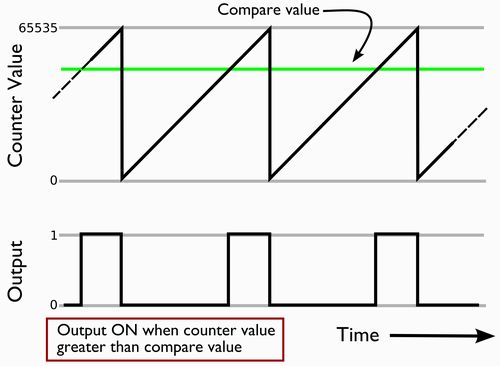
Again, the counter goes from 0 to 65535, counting at 8 MHz, and resets when it reaches the upper limit– at a rate of 122 Hz. When the counter passes the value in the compare register (45000), the output turns high. The output goes low again upon reset. The resulting output waveform has about a 30 percent duty cycle.
If we then change the upper counting limit from 65535 to 32767, the counter goes through a complete cycle in 4 ms, so the clock frequency is about 244 Hz. Since the compare register is again set to one half of the upper counting limit, the duty cycle is again about 50 percent. The average value of the output signal can be varied from zero to 100 percent of the logical output level, and that change is made by varying the time width of the regular output pulses, hence the name “pulse width modulation.”
This method of digital to analog conversion is never going to be particularly precise, so using our full 16 bits of resolution to specify the duty cycle is somewhat silly. Instead, we’ll use ten bits, which gives us 1024 possible different output levels. By making that sacrifice in resolution, we can gain some speed. We set the upper counting limit to 1023, which means that we can complete a full counting cycle in only 128 microseconds, giving us a respectable output frequency of 7.8 kHz.
How to make it happen
Now we know what we want the timer to do, so it’s just a matter of making the chip actually do those things. We need to (1) set the clock source and divider, (2) set the upper counting limit, (3) set an initial value for the compare register (perhaps equal to the upper counting limit), and (4) set the timer control registers as to make it operate in the mode that we have described. We’ll cover these in the most natural order, changing things as we come across them.
Let’s start with the clock. There are two, potentially different, clock signals that we need to worry about. The first is the microcontroller system clock frequency, and the second is the input signal to the counter/timer circuit. We will actually use the system clock frequency as the input to the timer so that these two frequencies are the same, but we will have to set it up to work that way
As we discussed earlier, we’re going to run the system clock off of the internal RC oscillator at its full rate of 8 MHz. It’s possible to run at a lower rate by using a clock prescaling divider, but we want to turn that feature off. The default clock configuration for the ATmegaX8 is to use the 8 MHz internal RC oscillator with a divide by 8 option (CKDIV8), resulting in a 1 MHz system clock. Changing this requires turning off the CKDIV8, which is in located in the Fuse Low Byte. The default Fuse Low Byte is #01100010b (01100010 in binary) or 98 in decimal, where the first bit controls CKDIV8. Changing only the first bit, we get #11100010b, or #226 decimal. (How to program the fuse bits depends on your specific programming environment.)
Next, we need to take care of choosing the clock source for the timer. The 16-bit timer documentation is in chapter 14 of the datasheet, and the clock source is controlled by “Timer/Counter1 Control Register B,” or TCCR1B. Here is what TCCR1B looks like:
| Bit | 7 | 6 | 5 | 4 | 3 | 2 | 1 | 0 |
|---|---|---|---|---|---|---|---|---|
| Bit Name | ICNC1 | ICES1 | —– | WGM13 | WGM12 | CS12 | CS11 | CS10 |
| Initial Value | 0 | 0 | 0 | 0 | 0 | 0 | 0 | 0 |
The lowest three bits are named CS10, CS11, and CS12, for Clock Select [counter] 1, bits 0-2. From table 14-5 in the data sheet, we see that these three bits should be set to 001 (decimal #1) to use the system clock ( called “I/O clock” here) without any prescaling divider.
What else is in TCCR1B? Bits 6 and 7 are for using the timer to measure external signals. We won’t be using those, so we can leave the default values of zero. The other two bits in TCCR1B that do something (WGM12 and WGM13) are control bits for the timer mode. They are two of the four control bits for the Counter/Timer “Waveform Generation Mode,” where the other two bits appear in one of the other control registers. From table 14-4, the mode that we want to use is fast PWM where the counter increments unidirectionally from 0 to a settable maximum value ( “top” ), and then starts over at zero, mode number 14.
The binary value for this mode is #1110b (decimal 14), so WG13 and WG12 should both be set to 1. Putting it all together, we want to set TCCR1B to #00011001b, or 25 decimal. In C, the code to set this register that way is just this: TCCR1B = 25;
The other half of the Waveform Generation Mode settings are held in (surprise) “Timer/Counter1 Control Register A,” or TCCR1A:
| Bit | 7 | 6 | 5 | 4 | 3 | 2 | 1 | 0 |
|---|---|---|---|---|---|---|---|---|
| Bit Name | COM1A1 | COM1A0 | COM1B1 | COM1B0 | —– | —– | WGM11 | WGM10 |
| Initial Value | 0 | 0 | 0 | 0 | 0 | 0 | 0 | 0 |
First, we want to set the two remaining bits of the Waveform Generation Mode, setting WGM11 to 1 and WGM10 to 0. The four highest bits of TCCR1A control the “Compare Output Mode” for each outputs A and B. As we said earlier, we want to choose a mode where the output turns high when the counter value equals the value in the compare register. From table 14-2, the setting for that mode is #11b for each of the two registers, making the four high bits of TCCR1A all equal to one. Putting it all together, we want to set TCCR1A to #11110010b, or 242 decimal. In C, the code to set this register that way is: TCCR1A = 242;
At this point we’ve set up the system clock frequency, the timer clock frequency, and we’ve set the output and compare modes appropriately. Because we’ve chosen waveform generation mode 14, the top value where the counter resets is given by the value stored in ICR1, the input capture register.
One needs to be a little bit careful setting ICR1, as well as the compare registers, because they are true 16-bit registers, and the high and low bytes must be written in the correct order if doing so through assembly language. Your C compiler, however, should take care of this for you:
ICR1 = 1023;
All that remains is to set the compare registers OCR1A and OCR1B to values that will set the duty cycles for the two outputs. Let’s start by setting output A to 50 percent and B to 80 percent duty cycle. (Note that 80 percent duty cycle means that the output turns on after 20 percent of the cycle.)
Then, we have
OCR1A = 511;
OCR1B = 204;
The last detail
Great! We’re done, right? Not quite. We’ve set up the timer to work correctly, but we haven’t yet told our microcontroller that it should actually output the signals from the timer. (Doh!) As we said earlier, OC1A and OC1B are located on pins 15 and 16 respectively. These pins are not dedicated for use with the timer, instead they are shared with the “Port B” set of general purpose I/O pins, and specifically with pins PB1 and PB2. Whether an individual pin is configured to be an input or output is controlled by the Port B Data Direction Register, DDRB, an 8-bit register that has a 0 (input) or 1 (output) for each of the eight pins in port B. DDRB defaults to all zeros, so that all of the pins are inputs. In order to use pins PB1 and PB2 as outputs for the timer, we will have to set them to be outputs, as is discussed in section 12.3.2 of the datasheet. To do that, we will set DDRB bits 1 and 2 (for PB1/OC1A and PB2/OC1B), and keep the others at zero, giving us
#00000110b, or 6 decimal. The C code for this is DDRB = 6;
A slightly nicer way to do this is to use the avr-libc macro _BV(bit), which is equivalent to the C command 1<<bit, except that it executes at compile time, so that it does not waste time computing the bit shift while the microcontroller is executing its program. (Read more about this macro here.) We could then write our C command as
DDRB = _BV(PB1) | _BV(PB2);
where PB1 and PB2 are defined as 1 and 2, respectively in io.h. The statement is then equivalent to DDRB = (1<<1) | (1<<2) = 2 | 4 = 6, but has the advantage of being somewhat easier to change than a hard and fast number like “6.”
The totality of our code, to generate the two pulse-width modulated signals with 50 percent and 80 percent duty cycle is as follows, and it looks pretty short:
TCCR1A = 242;

TCCR1B = 25;

ICR1 = 1023;

OCR1A = 511;

OCR1B = 204;

DDRB = _BV(PB1) | _BV(PB2);
After programming the device with this code– making sure to set the fuse byte as we discussed earlier– I looked at the output on my scope.
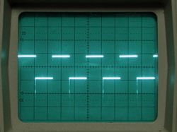 The signal shown here is the one with 50 percent duty cycle signal; you can see that it looks like a square wave. With a scale of 20 microseconds per division, I measured the period to be about 126 microseconds, giving a frequency of 7.94 kHz, which is within one percent of the nominal 8 kHz that we were expecting. (That’s pure luck: the datasheet only specifies that it’s good to within ten percent.)
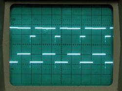 Here we have both the signals with 50 percent and 80 percent duty cycles.
The signal with 80 percent duty cycle is a little less clean; it jumps a little bit when the other signal (50 percent duty cycle) turns on– presumably because I’m driving LEDs with the timer outputs that are drawing substantial current. In any case, that causes a little bit of cross talk between the two output signals. (That needn’t be the case if you’re more careful than I was with your output signals.)
Thus far we have demonstrated making and driving pulse-width modulation signals. If you’re just trying to dim an LED with this technique, you can stop here, because your eye cannot detect the 8 kHz flashing. Otherwise, let’s go ahead and filter the output. Let’s start with a basic RC low-pass filter, aiming for a roll-off frequency of order 140 Hz . (I chose a 0.22 microfarad cap and a 33 kOhm, because I had those handy.)
On the left are the two input signals on the scope, with the inputs DC coupled, 2 volts per division and centered at bottom of screen and the middle. One signal is giving about 2.5 V output, the other about 4 V; quite reasonable estimates of 50 and 80 percent of 5 V. the picture on the right shows the AC ripple on those two signals, at 20 mV per division. While that’s fairly low already, you can filter more aggressively as needed.
Finally, we want to make a very, very simple function generator, just by varying the output compare value that is set in the timer. As a demonstration, here’s the code to produce a complimentary pair of 5 Hz triangle waves:
unsigned int m,n; //16-bit unsigned integers
unsigned char countingup;
TCCR1A = 242;
TCCR1B = 25;
ICR1 = 1023;
DDRB = _BV(PB1) | _BV(PB2); /* enable OC1A and OC1B as outputs, sums to #6 decimal. */
m = 0;
countingup = 0; //1 for increasing, 0 for decreasing
for (;;) // main loop
{
n = 0;
while (n <= 100U) //Change the length of the short delay here.
{ asm(“nop”);
n++;
}
if (countingup){
if (m < 1023)
m++;
else { m–;
countingup = 0;
}
} else { if (m > 0)
m–;
else {
m++;
countingup = 1;
} }
OCR1A = m;
OCR1B = 1023 – m;
} //End main loop.
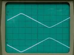
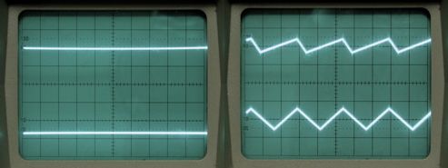
And on the scope it looks like this:
(It works!) So, that’s that: A simple, but potentially useful function generator. Imagine putting a couple of knobs (controlling voltages into the analog to digital converter inputs) in place to control amplitude and frequency, and you might even make a useful benchtop device. The sawtooth and square waves are left as exercises to the reader, and a higher frequency sine wave for the advanced students.

The _BV(bit) macro expands to exactly (1 << (bit)), as documented in avr-libc. You can use the macro for convenience, but it’s not magic. The avr-gcc does a great job evaluating constant expressions at compile time.
As another example, some of the functions in <util/delay.h> take "double" floating-point parameters. As long as you call these with constant compile-time values, your object code will not contain any floating-point code.
Use PSoC problem solved.
Not available, no free compiler, bloody expensive and complex.