


I took some close-up pictures of LEDs to get a look at what’s inside. These are just standard T-1 3/4 (5 mm) package superbright LEDs with clear lenses, one of the most common types, and I took the photos by placing my the lens of my camera (Canon S3 IS) right up to them.
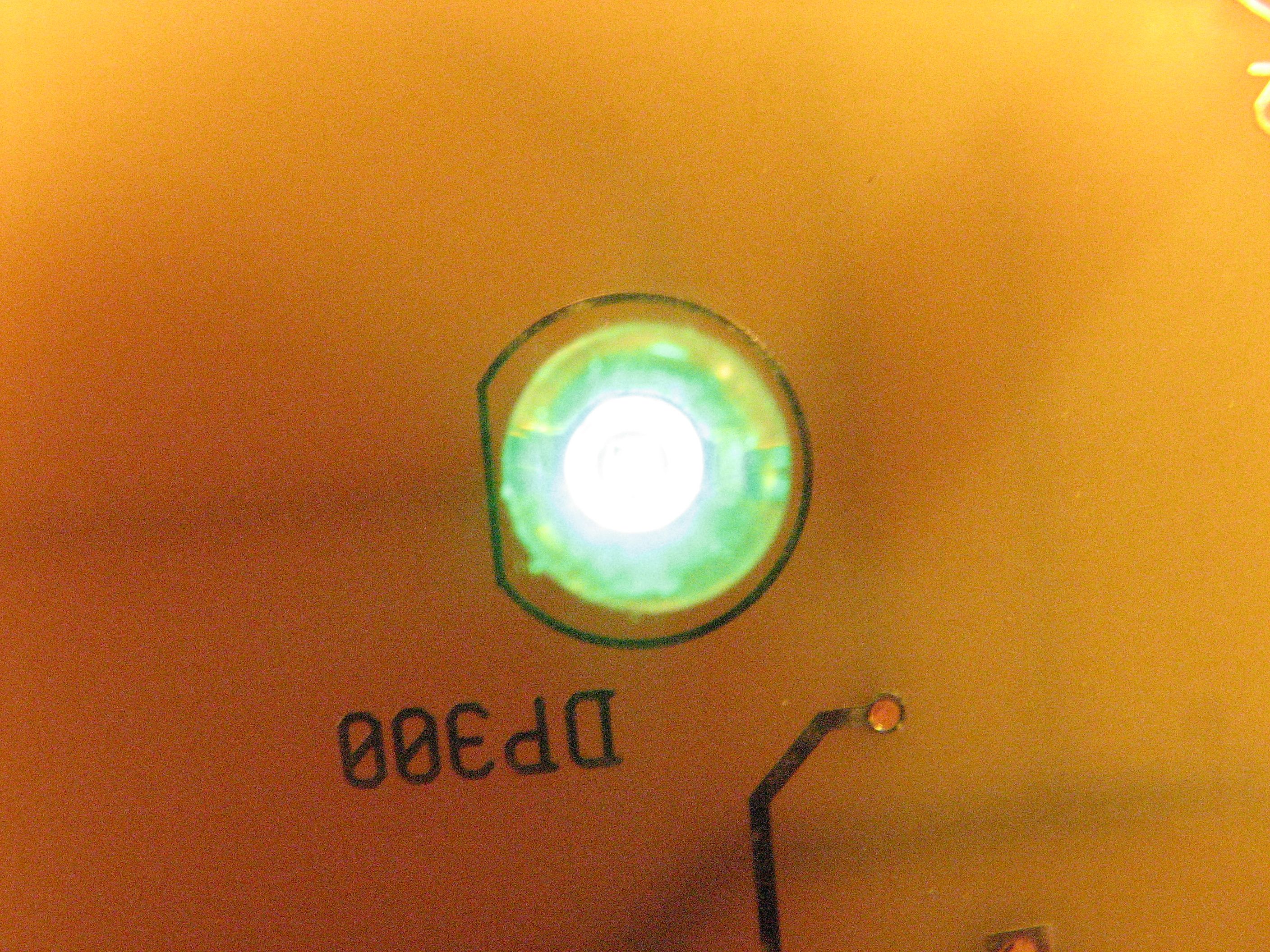
The first photo (above) shows what one of these LEDs looks like in a short but fairly normal exposure with good lighting. While this particular LED is a blindingly bright pure blue-green color, it’s interesting that the brightest part shows up as simply white in the photograph. Your eye can perceive something to still be blue but very bright, but that can’t actually be represented in a digital photo, except perhaps with an HDR technique. This oddity is a form of saturation phenomenon; one of the ways in which photos of LEDs typically misrepresent how they look like in real life.
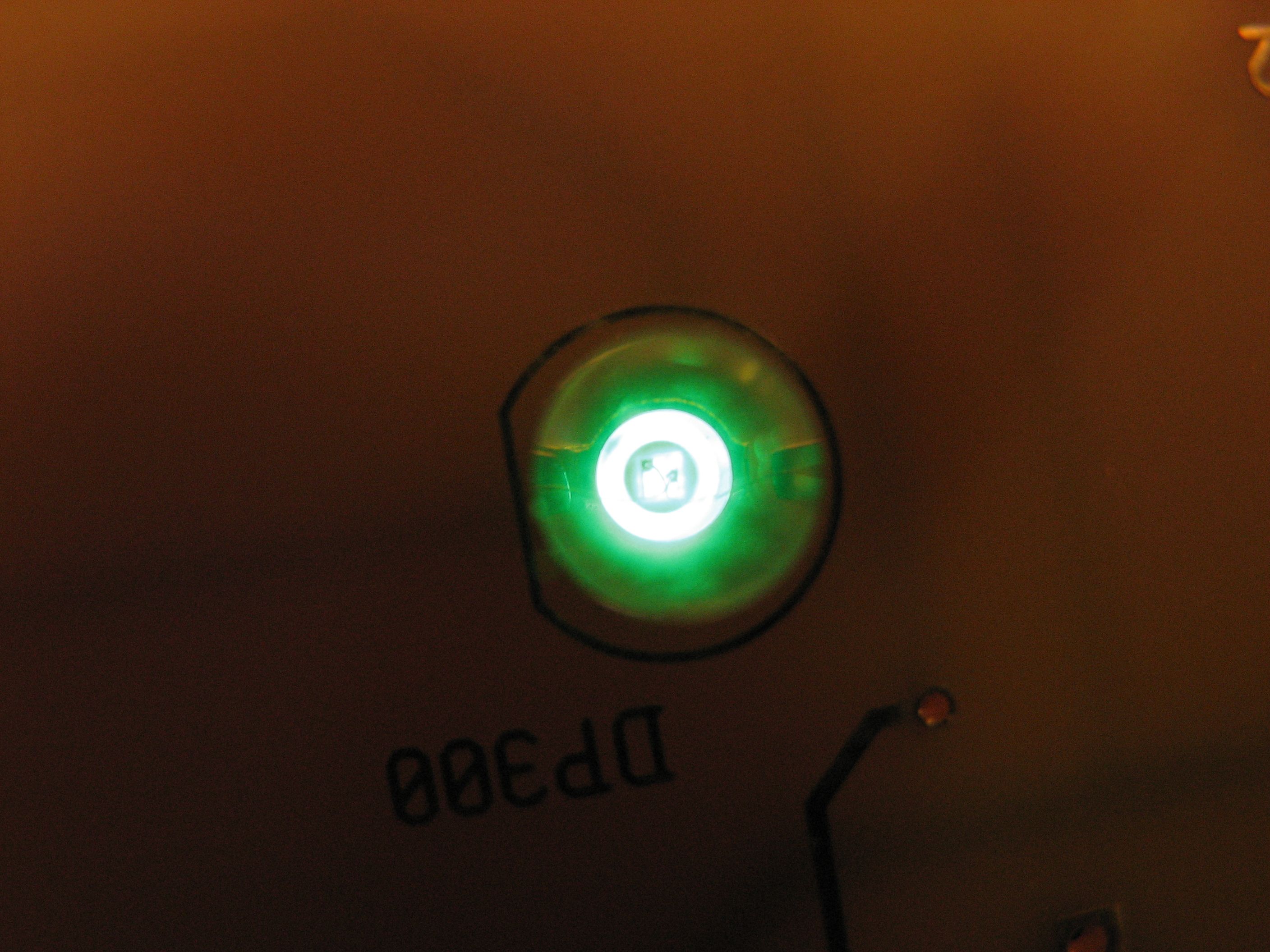
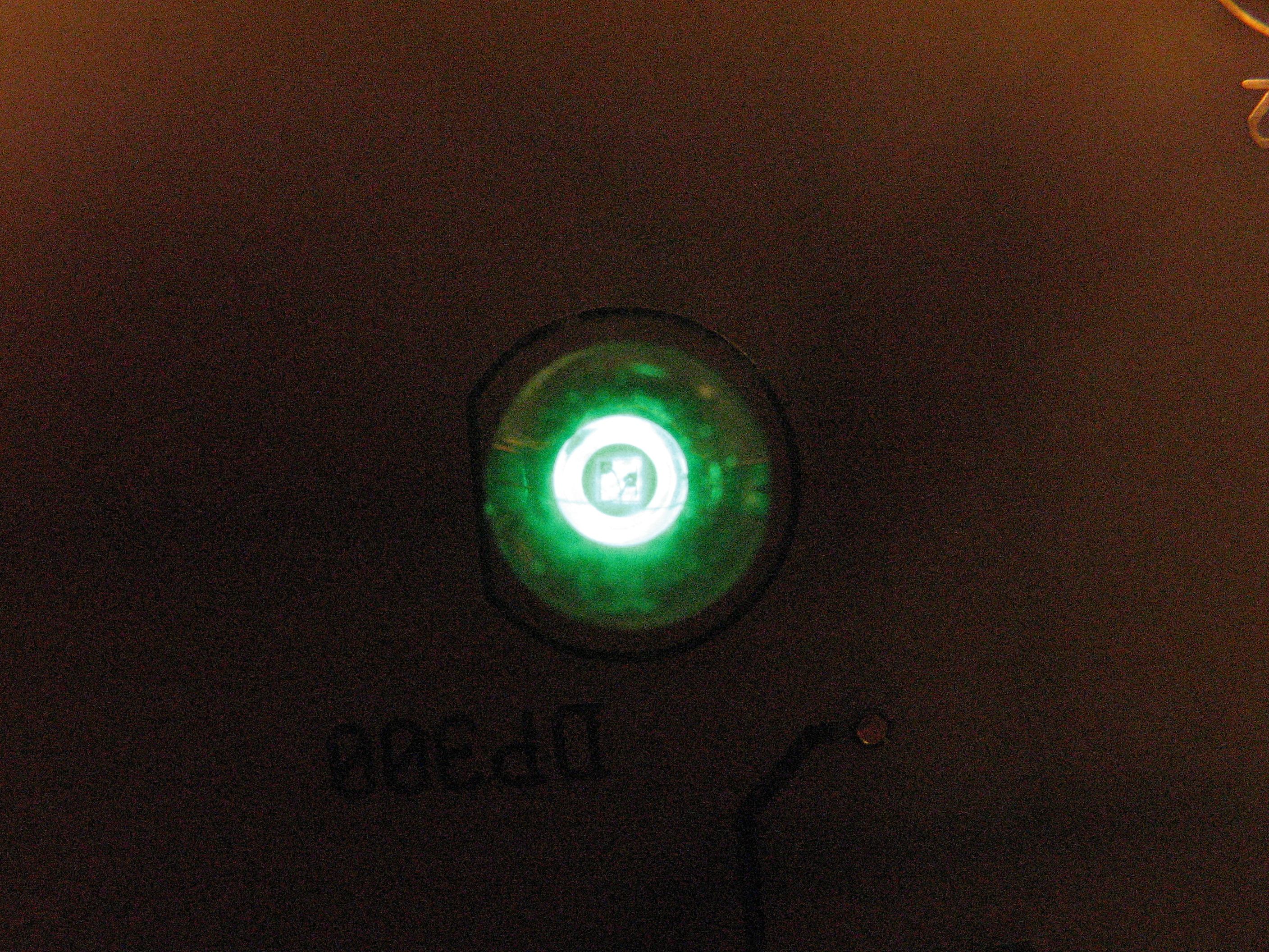
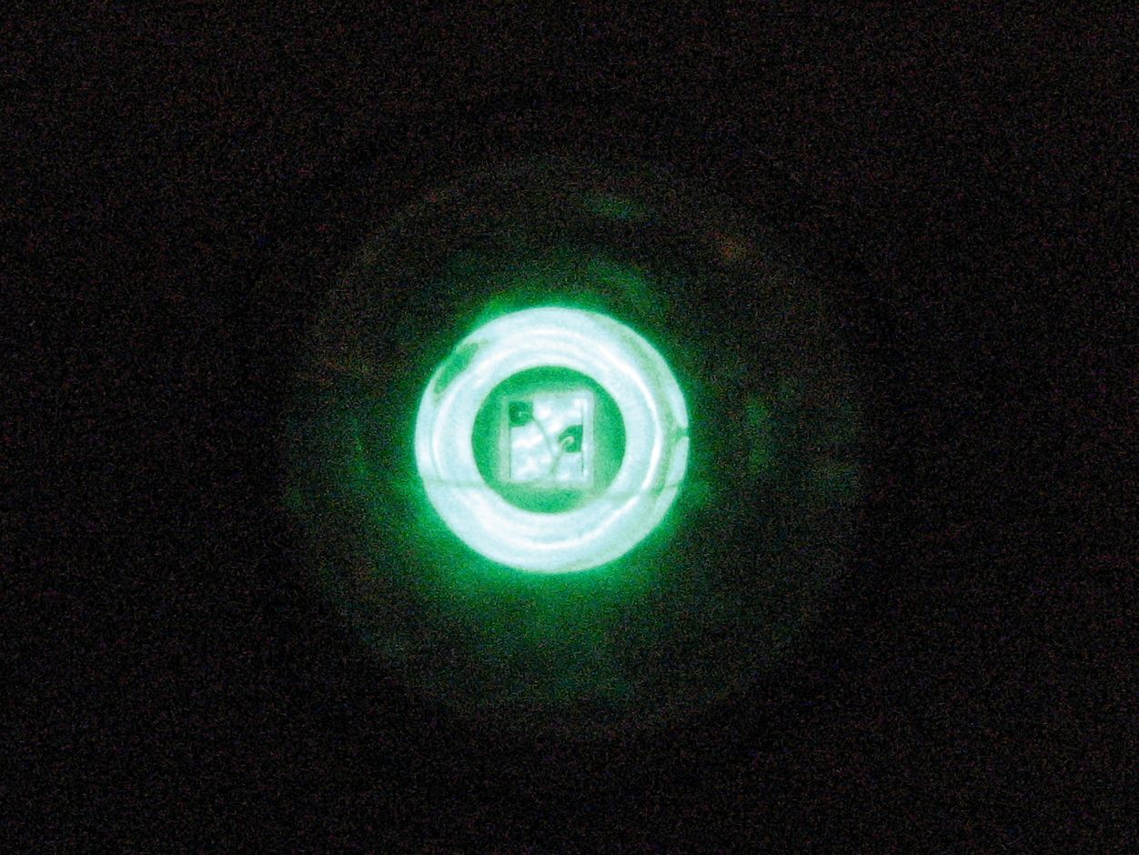
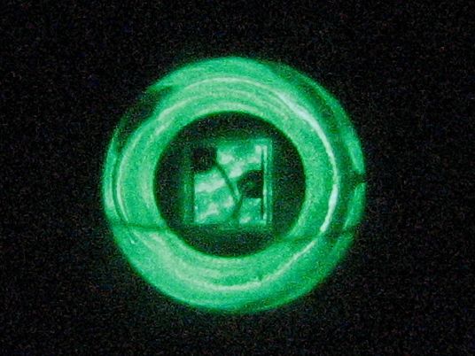
As we turn down the exposure and zoom in, the details of the LED begin to emerge. On this particular one, you can see the square chip of the LED and the reflected blue-green light around the edges of the plastic package. On top of the chip are two nearly microscopic wire bonds connecting the LED chip to the leads of the device.
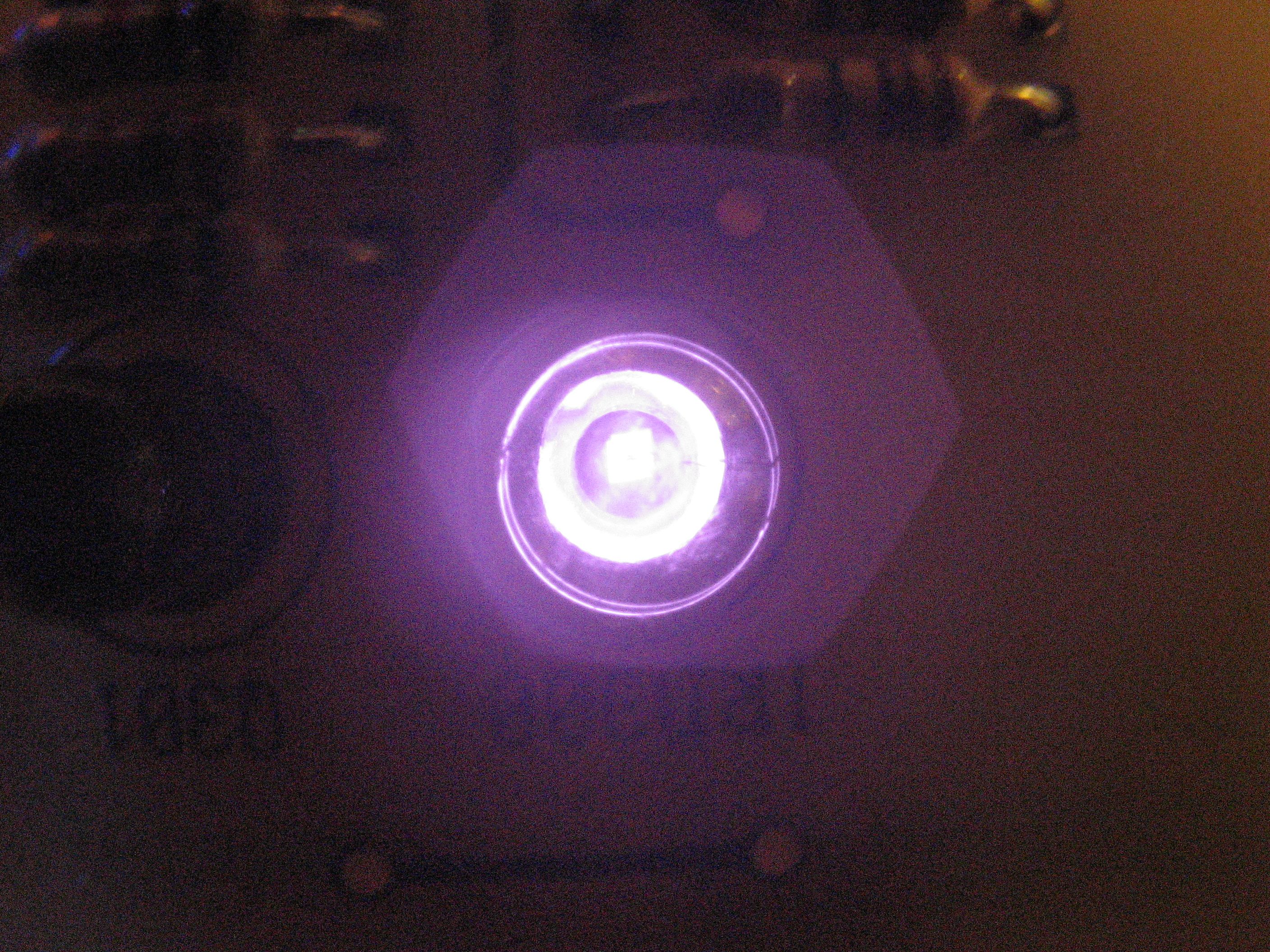
Next up, an infrared LED. Not too much interesting to look at here, but it is always interesting to see the light from an IR LED– which human eyes cannot see.
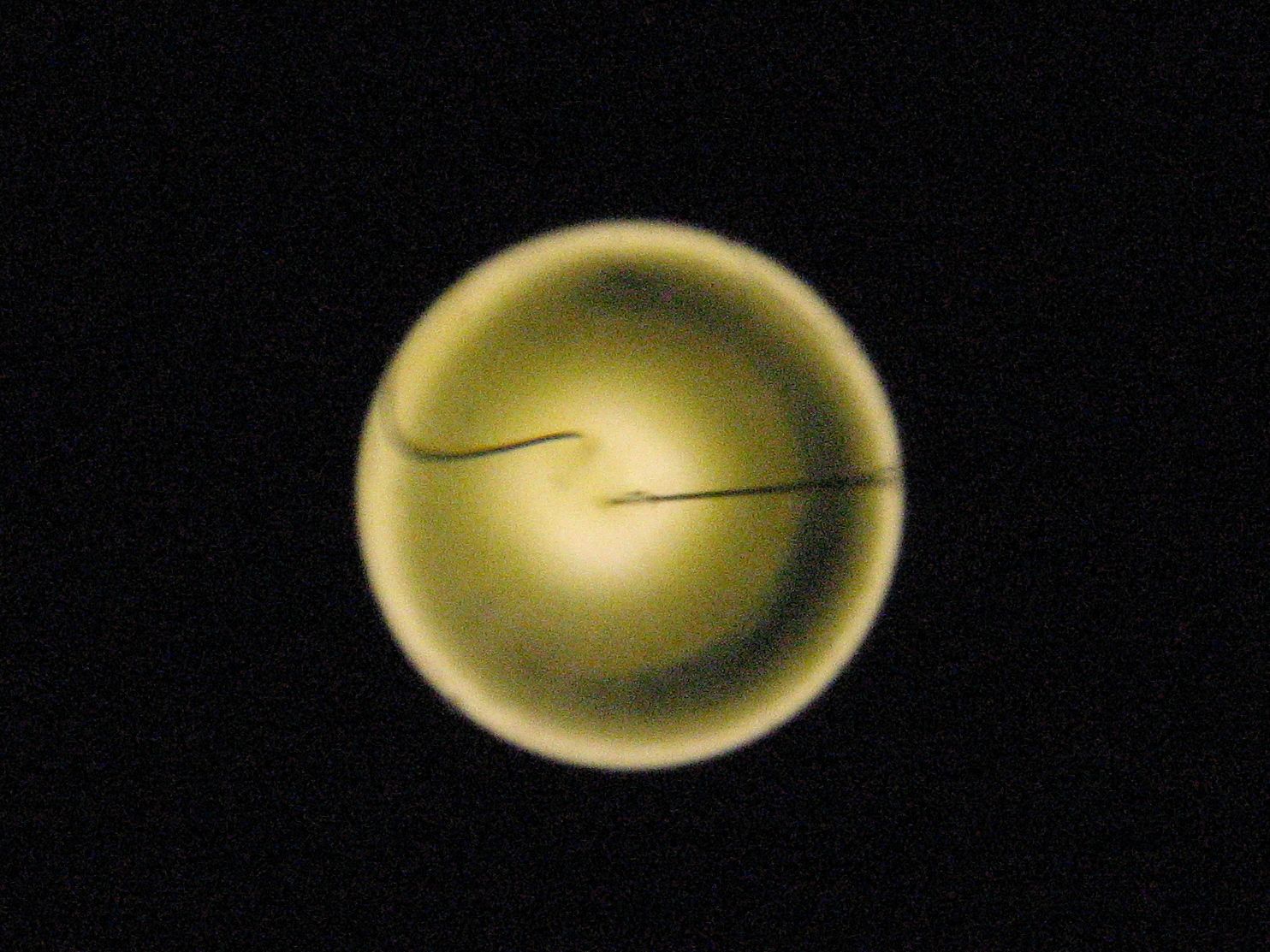
A white LED is an entirely different matter. Rather than a simple device like the green one, it’s actually a blue LED that illuminates a phosphor. While we can still see the two wire bonds, they seem to disappear into the phosphor, rather than remaining visible all the way to the chip.
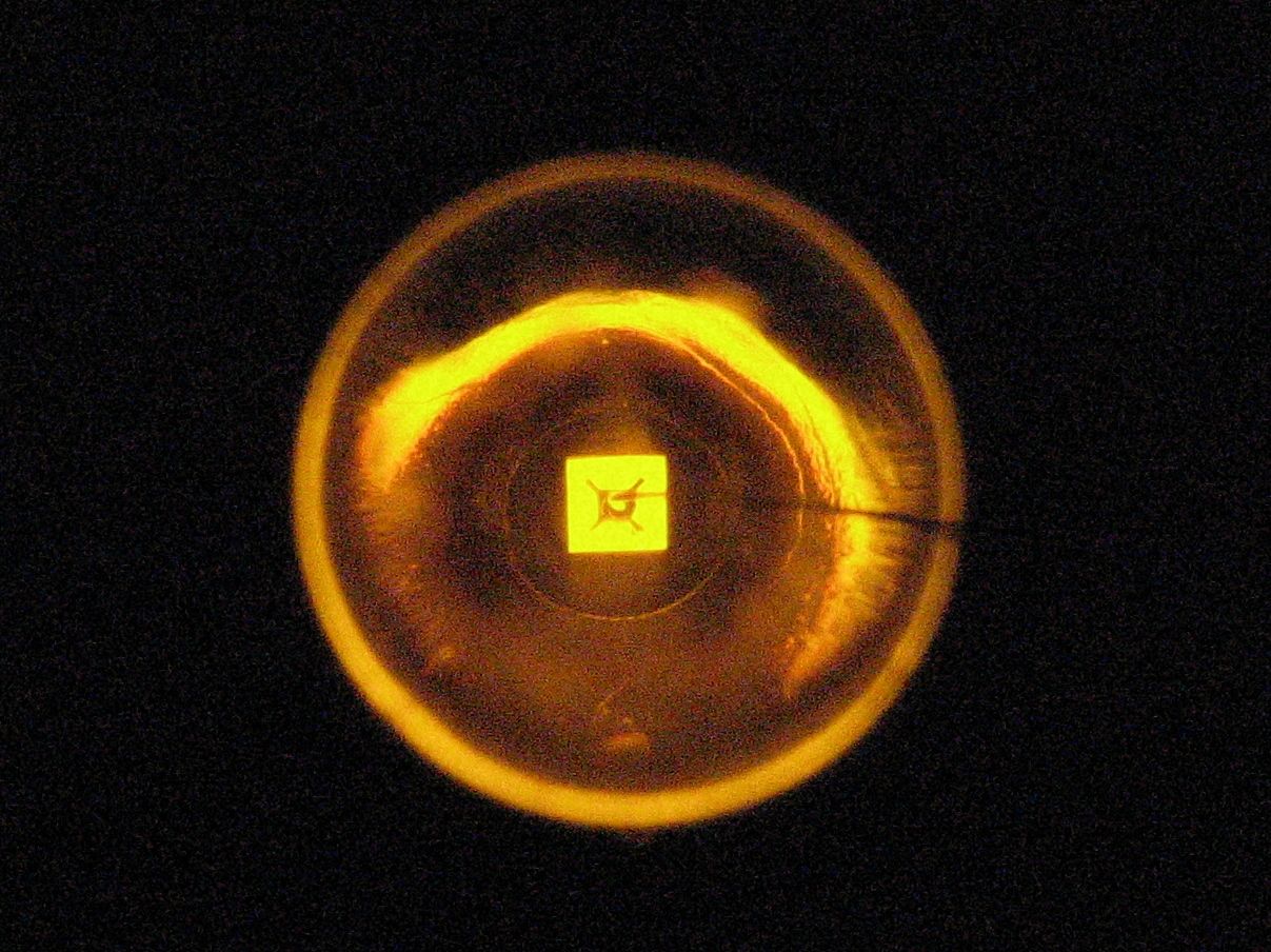
Finally, this orange LED has a slightly more traditional design where we only see a single wire bond. Its construction is a little bit like the one in this photo. The square structure in the middle of this photo is actually a metal reflector cup. The LED chip itself is actually very small and hard to see in this case– it’s the little black square in the middle, at the very end of the wire bond. Update: Thanks to some of the comments here, I went back and looked closely at this one by eye– I was wrong. The square in the middle is indeed the chip.
I’m pretty sure the entire bright square is the die in the amber LED, as the dark X shape is a part of the contact that is attached to the die. It would have to be a fantastic reflector to make a square shape that perfect… the reflector makes that vaguely semicircular gleam around the top part of the LED.
I agree to this, the square is the whole die. You have to keep in mind that you’re looking through a lens (the LED body). I think the die of such LEDs are about .3 x .3mm².
To get the real size you might get rid of the plastic, or at least you should cut/grind/polish the lens-part of the body of to take a picture through an even surface.
So far I know the X is used to get a more constand current flow through the whole die. Thios avoids high current denses in a small point (where the bond wire connects the die). That what the manufacturers say in their white papers ;-)
As another method of seeing the insides of an LED – larger and in real time – I once tried to check the cleanliness and circularness of a pinhole I had created for a pinhole camera by shining an LED thru the hole and on to a wall. It clearly showed the interior structure:
Here’s a quick link to the photo
Holy cow does that work well!
—
Windell H. Oskay
drwho(at)evilmadscientist.com
http://www.evilmadscientist.com/