


There has historically been, and still is, a lack of good, free MacOS native EDA (electronic design automation) software. The situation has somewhat improved in the past few years because the X11 layer in Mac OS X allows graphical unix applications to run natively on the Mac, concurrently with other programs. I recently learned to use some of these tools in the gEDA suite to lay out printed circuit boards. These (loosely, if at all, organized) notes should be helpful to anyone that wants to get started making PCBs using a mac, linux, or other unix-like system.
I use both fink and darwinports (which is renaming itself macports ) to install unix software on my Mac, although I’ve come to prefer fink.. These systems are effectively package managers, much like those found in various linux distributions, which can– in principle– automatically install all of the software parts that are required to install a major application. Some earlier documentation of this setup exists, but this installation is not all things sweet and light, so I thought I should put my two cents in.
Why bother? Because I want to be able to design PCBs with free, accessible, tools. Yes, Eagle is very popular, and available on multiple platforms but it is not free. Other commercial layout packages can easily reach into the tens of thousands of dollars.
The open source project gEDA is coming along nicely and is already quite viable on some platforms. With some work– documented below– I was able to get gEDA tools to compile on my mac, and use it to design some large boards.
When I first started looking at open-source tools for PCBs, I came across names like gEDA, xcircuit, and pcb, not really knowing their relationships.
I installed xcircuit using darwinports; it may also be possible to build it directly. Once it’s installed, open up an X11 terminal window and enter “xcircuit &” to launch it. My first impression of xcircuit is that it seems very primitive. But, thinking about it, every piece of EDA software that I’ve ever used has seemed primitive. Often, the more expensive the tools, the more primitive they seem. There’s a tutorial for xcircuit here. (Eventually, I decided that xcircuit was not for me, opting for gschem, part of the gEDA suite instead.)
I was able to install pcb by compiling it directly, without using fink or darwinports. However, it was not quite working quite properly– the window management was somewhat screwy. However, that’s exactly why you want to use the package manager– so you don’t foul something up because you forgot to check something important that you didn’t know about.
Which brings us back to Fink. Recently, a number of EDA tools have become available through Fink, and this excellent page summarizes how to install them. First, install fink if you haven’t done so already. To install the major gEDA tools you enter fink install geda-bundle in the terminal. Fink will ask for your password and then download and install the necessary software bundles.
Or, at least it’s supposed to. Mine crapped out with error message ‘Failed: Can’t resolve dependency “transfig (>= 3.2.5-1004)” for package “geda-symbols-20050820-1004” (no matching packages/versions found).’ Doh. The problem is that the current fink package of transfig is at version 3.2.4-6, but version 3.2.5-1004 is required. An alternate version (transfig-graphicx 3.2.5-1007) is available, so I installed it as follows: fink install transfig-graphicx.
This worked, and installed transfig-graphicx 3.2.5-1007, but even so, I couldn’t install gEDA. So what’s going on now? Run fink list -i to see the list of installed packages. This turns up not only transfig-graphicx 3.2.5-1007, but also a “virtual package” of transfig 3.2.4-6. (Double doh!)
Transfig is part of xfig, the drawing program, and you can download components of it here. I downloaded transfig.3.2.5_alpha7.tar.gz
Backing up a bit here… and as our president says, using “The Google,” I found this page by Mikey Sklar, who has his own fink install scripts and instructions for exactly this problem. I would add to his instructions the followings warnings: This takes approximately a whole day to install, you should have a broadband connection to download the files, and a few GB of disk space to burn. The principal operation of the installation is a command line operation, fink -y install geda-bundle. This attempts to install the entire geda-bundle and uses the “-y” option, which automatically says “yes” to the default option when given any choice during the install.
After about four hours and 1.5 GB, this set of scripts finally crapped out and said “Failed: Problem resolving dependencies. Check for circular dependencies.” The trouble is, I didn’t want to spend all day sorting out dependencies, which is why I’m trying to install this by using someone else’s install scripts!
The geda-bundle consists of a list of packages to install. To check if the first package (geda-doc) had installed correctly, I entered fink install geda-doc, which either attempts to install it or returns a message (“No packages to install.”) indicating that the package is already installed. It turned out that the first two packages (geda-doc and geda-examples) had installed correctly, but something had gone wrong on the third package, geda-gattrib. When I tried to install this component by typing
“fink install geda-gattrib,” I was presented with a choice: fink needs help picking an alternative to satisfy a virtual dependency. The candidates:
(1) libgeda26-data: GNU EDA — Electronics design software — data files
(2) libgeda27-data: GNU EDA — Electronics design software — data files
Pick one: [1]
The default choice (libgeda26-data) led to the error, so I tried option 2 (libgeda27-data), which worked and allowed geda-gattrib to install correctly. That issue resolved, I again entered “fink -y install geda-bundle” to try to install the rest of the components and– everything else worked. (Whew!)
There’s one remaining loose end to tidy up, which is to make sure that the system paths are set correctly for software installed by fink. The paths tell the system where to find the programs when you try to launch them, so if your gEDA programs don’t launch, make sure that these are correct. If you read the instructions when you installed fink, you’ve probably already set this up. If not, or if you want to double check, follow the instructions under the heading “Setting Up Your Environment” in the fink installation procedures.
Starting to work with gEDA:
The gEDA documentation wiki is the primary source of documentation. gEDA is not a single program but a collection of programs. If you’re new to printed circuit design, you need to learn some vocabulary in order to navigate around the different programs. Loosely speaking, you use a schematic capture program (gschem) to make a circuit diagram that can export a data file of wiring connections, called a netlist, to the layout program (pcb), which you use to actually design the board. Once the board is designed, you can export the design as a set of gerber files that can be sent to a PCB manufacturing service. The gEDA documentation has a sort of flowchart to explain this on this page.
To start building your schematic, launch gschem by opening up an X11 terminal window and entering “gschem &”. You might want to start by adding a component, by selecting “Component” from the “Add” menu, which seems straightforward enough. As much as I’d like to then say “just play with it,” as I usually do for new software, that’s actually the wrong approach here. Every set of schematic and layout tools that I’ve ever used has seemed like a program from fifteen years ago, and this is no exception! You should start with this gschem warmup and proceed right to the full-blown tutorial on making a schematic and laying out the PCB. This article is a slightly more user-friendly version that covers much of the same ground.

Schematic capture in gschem
But hey, it works. Hints: You will need to map a footprint to each component to move from gschem to pcb. I found this hint to be helpful– open up a new session in pcb and start placing footprints to see what they look like.
Multi-part components are a little bit tricky and not yet supported as well as I would like to see. For example, in placing an LM324 quad op-amp you need to edit the “slot” of each part to indicate which part of the op-amp that it’s from. That’s fine, but when you run the refdes_renum program to auto-update the reference labels, it set the four op-amps to come from different chips. Then you need to go back go gschem to tell it that, yes, those four are actually all part of the same chip.
Overall, I would rate the combination of gschem and PCB as usable but not anywhere close to user-friendly. One of the biggest problems is that there’s isn’t any real documentation from a casual user’s point of view. There’s the tutorial in getting started that I mentioned, and there is the (hardcore) official documentation, which has a grand total of three-count-em-three images in its 130+ pages. Dude, it’s a graphics program; we need pictures! Anyway, the documentation is probably very useful if you are a developer working on improving the program.
Minor annoyances are easily found; the board optimizing features sound great but do not really seem to do much of anything. Scrolling to the edge of the screen while dragging a component slowly scrolls: good. Scrolling to the edge of the screen while drawing a wire does nothing: bad, inconsistent, and illogical. It’s tricky to figure out how to move component labels; I still haven’t figured out how to move them between layers, although I seem to have done it accidentally exactly once. Once my grid stopped working– closing and reopening PCB fixed it. (Ugh.) Several other mysteries have also been resolved that way, and that is *not* a good sign. Really my fault but still annoying: my multi-page schematic failed to show up properly in the layout program because I entered the net names in the “netname” attribute field, instead of that for the “net” attribute. And then, the net name (not netname) “io42” does not work, but “io42:1” does– and I have no idea either why, or how I figured out to try adding the “:1” to the end, or why that should matter– the documentation leaves something to be desired. In almost all of these cases, a little bit of documentation would go a long way.
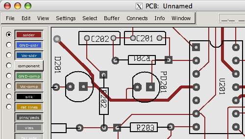
Laying out the board in PCB
Other hints: There is a built-in pseudo-help-like list of key commands for PCB, take a look. I wish that more of the commands were in the list– there are a lot of “secret” commands, or so it seems. About half of the available commands seem to be single-letter commands– and the list should be much more comprehensive and documented. One that you need to know: shift reverses the orientation of a new line.
I found gattrib, which can edit attributes of objects in the gschem files, to be unstable. It’s too bad– My circuit has four schematic pages with hundreds of components, and I realized after completing my layout that the holes drilled for *all of the resistors* were too small to fit the resistor leads. Doh! (You may want to carefully inspect the footprints in the libraries before using them.) In a situation like this, the right thing to do is to be able to quickly go through the schematics with a tool like gattrib to edit the footprint names in bulk. As it turned out, with gattrib broken, I realized that I could just open the schematic (.sch) file as a text document and do a search and replace on the footprint names– it turned out to be faster than gattrib would have been anyway.
One neat, excellent section from the documentation is the part on PCB Tips, which includes a trick to import external vector graphics to put on your board. You can use the wonderful utility pstoedit to convert graphics from (e.g.) Inkscape to PCB format. I did just that, to put our logo in the copper layer of our circuit boards:

Nice. =)
Finally, there’s another web site to look at that accumulates symbols for the gEDA programs. Logically enough, it’s called gedasymbols.org.

You might want to check out KICAD, a GPL’d schematic capture and PCB design suite. I’ve been using it the last couple of weeks, and it’s been a pleasure. Portions are still a little rough, but it remains highly usable. I already prefer it to Eagle.
Runs under Windows and Linux, unfortunately explicit support for OS X doesn’t seem available just yet.
Hey thanks– that looks really sweet! I’ll have to check it out.
-Windell.
—
Windell H. Oskay
drwho(at)evilmadscientist.com
http://www.evilmadscientist.com/
KiCad now has specific binary file support for the MAC. Check it out here:
Learning about KiCad
Thanks for the tip!
—
Windell H. Oskay
drwho(at)evilmadscientist.com
http://www.evilmadscientist.com/
Mine is crapping out for another reason. Ostensibly, due to the fact that it cannot find the package whatsoever.
CRAP!!!
Failed: no package found for specification ‘geda-bundle’!
Andy Ideas?
Thanks!
Chris L. – ñeurascenic
Without seeing your setup it is not really possible for me to debug it. Are you running the script by Mikey Sklar?
—
Windell H. Oskay
drwho(at)evilmadscientist.com
http://www.evilmadscientist.com/
plz can you give me the map of this circuit i wont to print it ??? my email maheralafndy@gmail.com
thanks
Sorry to necro-bump a post from 2007, but most of the discussion about gEDA and its user interface and user friendliness seems to have died out on here over the years.
Now that you’ve been using gEDA for so long (well, mostly gschem and pcb, I’d imagine), has anything improved since this article was written, or have you just gotten used to it enough that the little things aren’t as much of a hassle any more?
Actually, speaking of which, given that it’s been so long since this article was written, and I’ve seen some updates or mentions of gEDA in other posts, maybe it’s time to re-visit the topic as a fresh article?
Just curious. I’m thinking of delving into some circuit design stuff soon, and think it might be interesting to hear your current take on the open-source EDA field.
Of course, the "preview" is there to avoid stuff like an instant-reply-edit thing… sorry. :( But, wanted to pass along that I’m using a Mac, as well, which is part of why the original May, 2007 post caught my eye, and why I’m interested in new thoughts, if any are available, regarding the Mac open-source EDA scene.
Thanks, Windell! :)
I’m definitely still using gEDA, and it has gotten much better and much easier to install, through fink these days, without any hassle. A second mac-friendly option is virtualbox+ubuntu, which is actually faster to download and install than the fink bundle.
We’ll revisit it at some point. There have been a couple of longstanding features in development that should increase the appeal more widely, and I’ve been waiting for those to be released before making much more noise about it.
Windell H. Oskay
drwho(at)evilmadscientist.com
http://www.evilmadscientist.com/