


For all of our different AVR microcontroller based projects, we seem to find ourselves continually wiring up minimalist target boards; little circuit boards that fit both the AVR and a 6-pin header for connecting to your in-system programmer. And, when you find yourself hand-wiring the same circuit over and over again on a protoboard, that’s really just life’s way of telling you “just lay out a damn printed circuit board already.”
Coincidentally, we needed a new business card.
That’s a bit of an exaggeration; we didn’t need a new card so much as we were enamored with the idea of having a card that did something interesting.
We certainly aren’t the first to have that itch– people are already making interesting electronic or circuit business cards, and there was even a contest at Hack a Day to design circuits that would run on their business cards.
(Digression complete.)
Project goals
We’ve been designing a lot of things based on the ATmega168, and we didn’t want to wire up any more by hand.
(The ATmega168 is a popular AVR microcontroller; it’s the one found in the Arduino.)
Our design goals for this project were (1) to make a printed circuit board version of the minimalist target board for the ATmega168, encompassing a place for the chip and a connection to the 6-pin ISP header, (2) to make a minimal and inexpensive circuit board platform that you could use to deploy a single AVR somewhere with without much fuss, (3) to encompass the capacity of a breakout board, giving extra holes to tap into each pin of the AVR and provide labels for every pin, (4) to fit in some small amount of flexible prototyping space, (5) to make it all fit into a neat business-card form factor, and (6) to release it as an open-source project.
The Design
Here is what we ended up with:
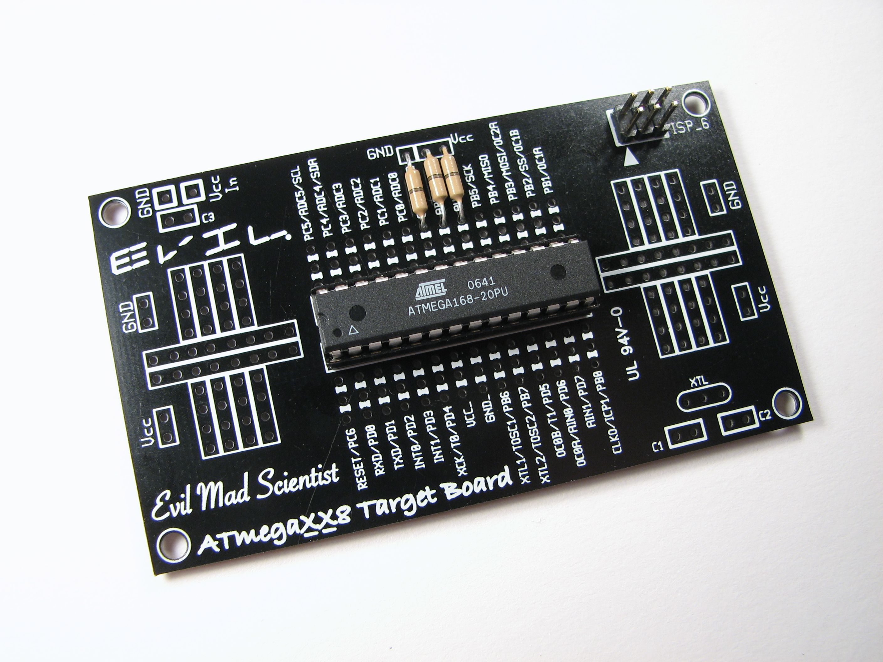
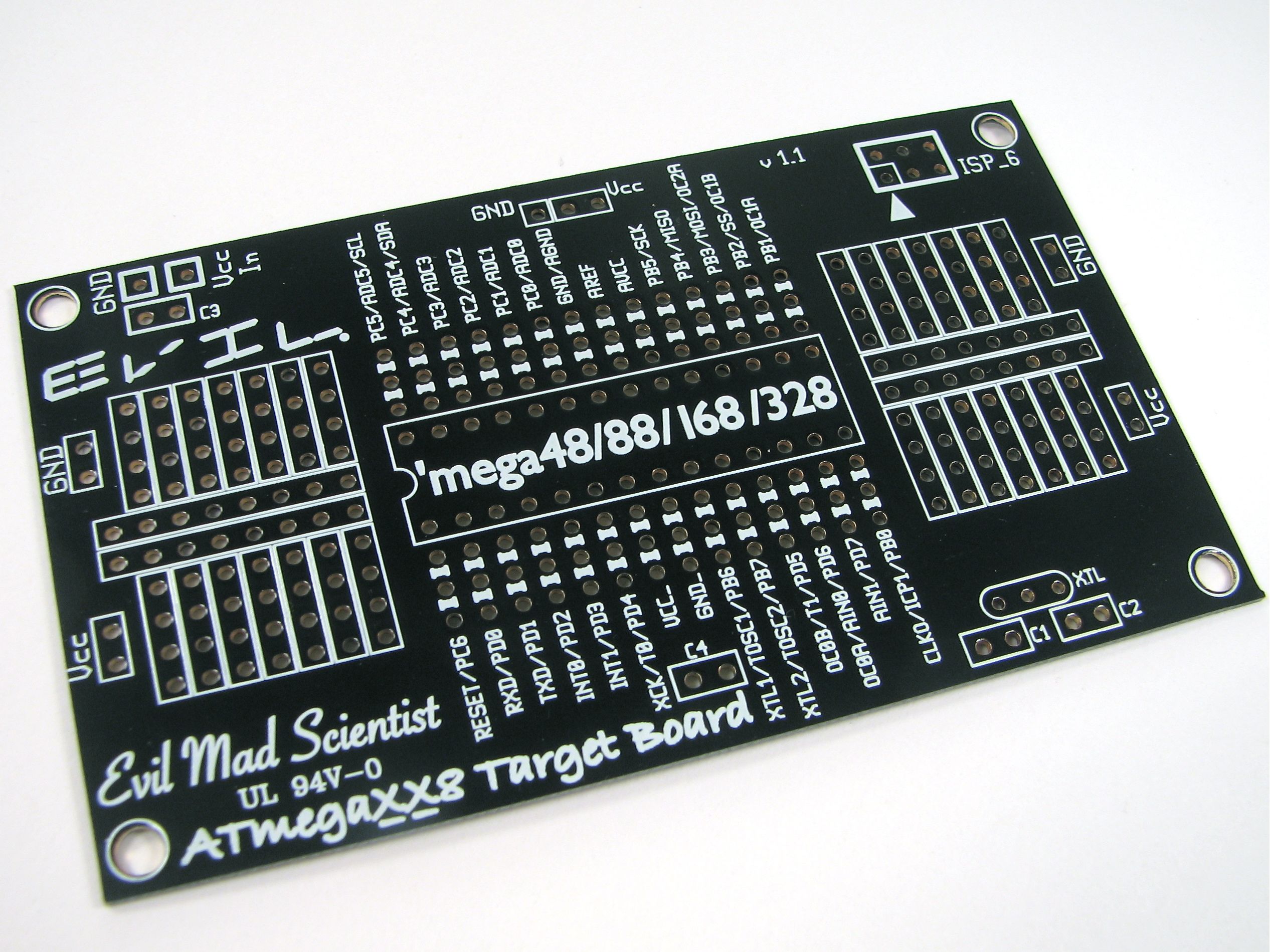
The circuit board is 2″ x 3.5″ (Standard business card size of course). It is designed so that all of the copper traces are on the bottom side, meaning that it can be built single-sided, either to keep the cost down, or to make it an easy design to fabricate yourself if you like to etch your own boards.
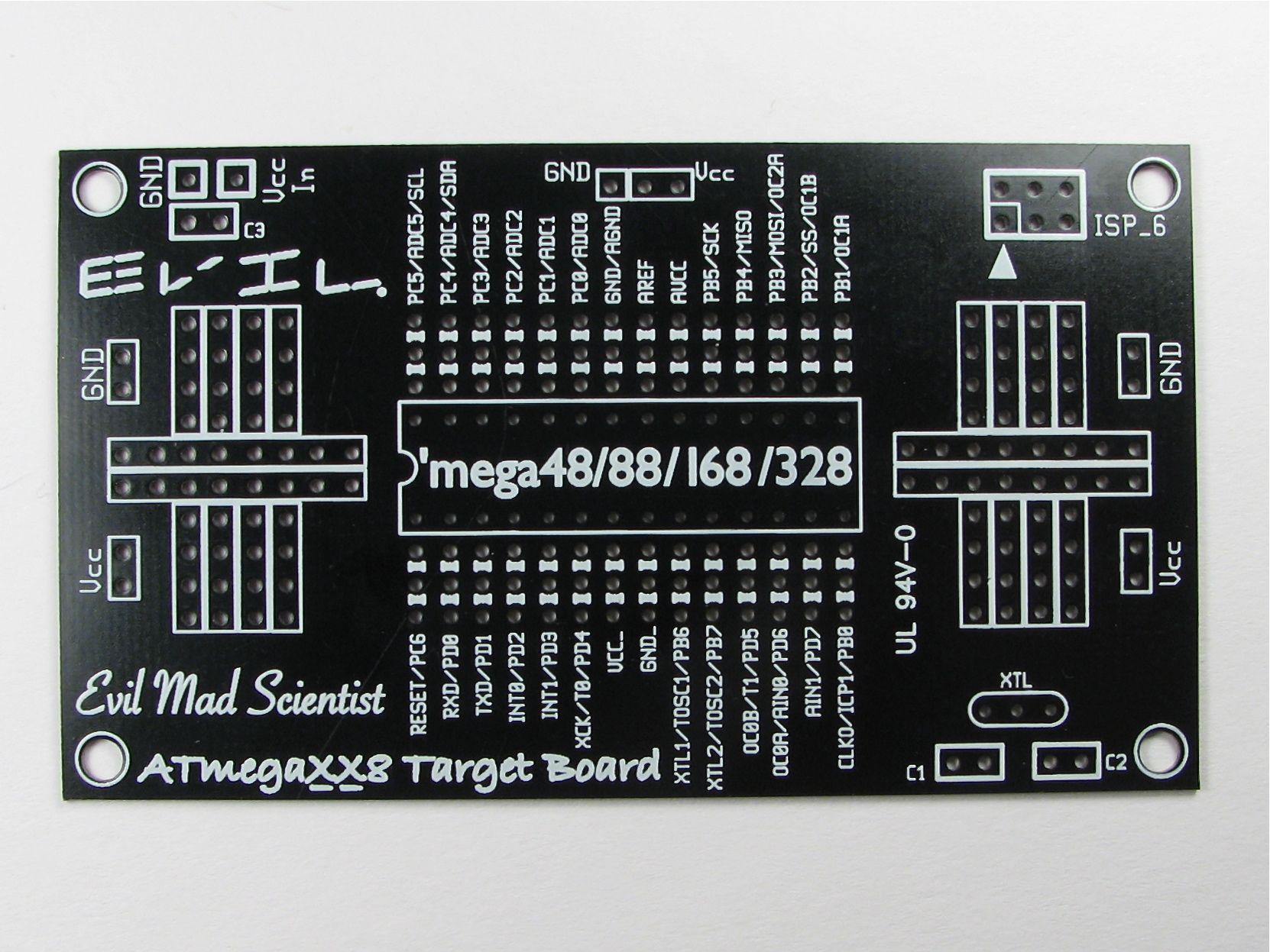
On the top side of the board, dominating the playing field, is the place for the microcontroller, which can sit in a standard DIP socket. While we mainly discuss the
ATmega168, it actually works equally well for the ATmega48, ATmega88, and the ATmega328P (if you can find a ATmega328P!), hence the designation ATmegaXX8 Target Board. The board is also compatible with the older ATmega8, although the feature set is slightly different from those in the 48/88/168 genus.
All 28 pins of the microcontroller are labeled with their main functions. Besides the pins that actually connect to the ATmega168, there are three-count-em-three extra access holes connected to every pin of the microcontroller. In the upper left, there are input connections for power (typically 3-5 V) and ground, which are routed to a couple of other locations on the board. In the upper right is a place for the 6-pin ISP header with pin 1 marked. In the lower right is a place to add an optional crystal oscillator with its two capacitors, or a 3-pin ceramic resonator.
On the left and right sides of the chip location are two breadboard-style prototyping areas, each with enough room for a DIP-8 package or the equivalent.
(Not that we could begin to scratch the surface of what cool things can fit in that space, but we might point out common op-amps or optoisolators for input or output signal conditioning, or even a pair of half-bridge drivers for controlling a motor. Or a
hexadecimal rotary dip switch. Or, from the obtuse-rather-than-useful department, use the space to add two more tiny AVR chips!)
This board does not have hardwired connections between the power and ground sections and the analog power section (AGND, VREF, AVCC pins), which allows you to substitute in other (or better) references to the analog section if you need them. If you’re happy with the standard analog-to-digital converter performance, or if you don’t use it at all, it’s recommended to jumper the pin AGND to ground and VREF and AVCC to the positive power supply, which are conveniently located nearby, near the upper middle of the chip. (See photo at the top of the page for an example with the jumpers in place.)
Finally, mounting holes are provided in each corner for 6-32 size screws, located with centers 1/8″ x 1/8″ from each corner.
Using the board
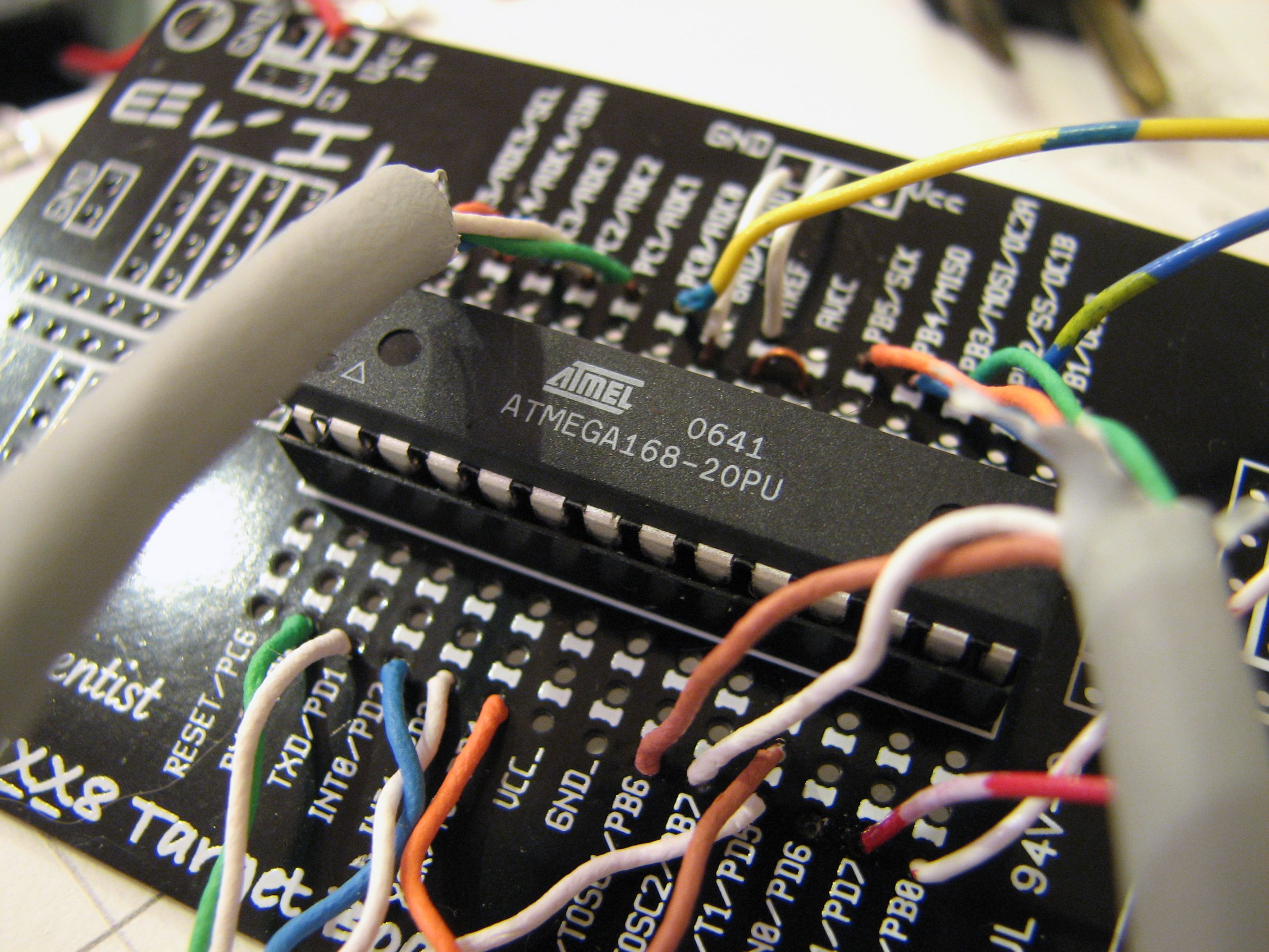
Since this is effectively an implementation of the minimalist target board, you don’t need much to run one of these. Ideally, the board, plus a chip, plus the 6-pin ISP header and a programming interface (at least once). To run on its own it will need and external power source as well, and AVRs like this can run (depending on load) from a 3V lithium coin cell or from a more powerful source. We usually run ours on external battery boxes with switches, either with two or three AA cells.
Under the hood
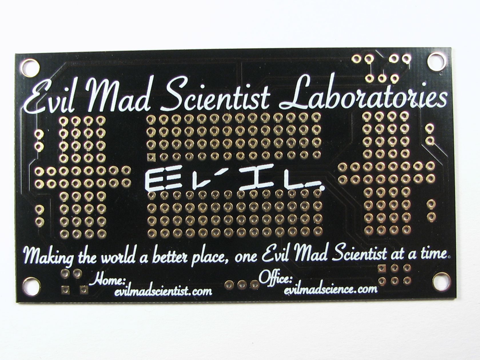
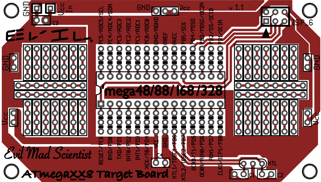
Again, this board is designed for easy single-sided fabrication; the copper layer, which goes on the bottom side of the board, looks like this:

To get started working with this design on your own, we have a single ZIP file, available for download here, (584 kB .ZIP file) which contains the full schematic diagram (PDF format), a PDF of the PCB layout showing the individual circuit board layers broken out individually with crop marks– making this layout a cinch even for home-etched circuit boards, and the original PCB layout file. (The circuit board was designed in gEDA PCB— free, open-source printed circuit board software.) We are releasing the design for this board under open source licenses and under a creative commons license as well.
Or, take the easy way out and get a kit here. :)
Want to talk about it? That’s what the forums are for.
Got projects based on this board to show off? We’d love to see your pictures in the Evil Mad Science Auxiliary.
Update:
New design for version 1.1 of the card (11/7/2008). The new version makes several changes. First, the microcontroller pin holes are now large enough to accommodate a ZIF socket. Next, we’ve extended the amount of prototyping space, so that there’s room for a DIP-14 socket on each side of the AVR (up from DIP-8 on each side). That means that you could fit, say, two quad op-amp chips on board! Third, we’ve extended the amount of “ground plane” copper on the bottom side of the board, and generally increased the width of ground and power traces wherever possible. Here’s what the new design looks like:
And here is a screenshot showing the new copper layer:
You can download the design files for version 1.1 of the card here, (768 kB .ZIP file) which again contains the full schematic diagram (PDF format), PCB layout, and layer separations.
(And of course, these are available at the Evil Mad Science Shop.)
That is just so cool. I wish I was you :(
To quote the folks at Guinness,
“Brilliant!”
What about adding two more holes very close to the MCU Vcc and GND pins, nicely spaced (300 mil) so one can add a 100nF decoupling capacitor?
With the current layout you can add a capacitor, but the then the capacitor is not neatly oriented in parallel with the MCU :-) I mean, this is a business card, and you don’t want to have any wrinkles in your card, do you? :-)
Similar for the reset pin. Some holes and traces to allow mounting a pullup resistor (if desired), a capacitor (questionable), a protection diode (seldomly done), and a reset switch would be nice.
And if you want to drive it over the edge, some holes and traces to mount a LM2940 voltage regulator, and two caps for power supply.
Okay, you’ve got some good ideas… but I’m not (necessarily) convinced that we need to add any of those things yet. There is plenty of room to put a good 100 mil 100 nF cap right across the power supply pins– it will fit neatly next to the chip– I don’t see a wrinkle there. What kind of giant 100 nF cap are you using? :)
(There’s also a spot "C3" for an input decoupling cap right at the power supply inputs.)
One of the reasons to put in those two big "breadboard" style area was to allow room for a full size reset button if you want one, and a pull-up will fit too. So… if that’s what you want to do with the prototyping area, great. We could potentially add a space for a tiny tiny buttons switch as well.
As far as voltage regulators, I’m afraid that I don’t see the motivation. It takes just as much off-board space to source appropriate voltage (3-5 V) as it does for an inappropriate voltage that would need a regulator– either with a battery or compact regulating power supply. Although, now that you’ve got me thinking about it… we could possibly add a spot to put one of the power jacks for the 4.5 V power supply, like we have on the Peggy.
—
Windell H. Oskay
drwho(at)evilmadscientist.com
http://www.evilmadscientist.com/
> What kind of giant 100 nF cap are you using? :)
Remark:
Well, for example most of TH < 1uf caps here (Czech Republic) have 200mil pin spacing, same as TH tantalum caps.
I love this business card is a brilliant idea very creative. I wich I could have one of this just in case someone want to give me one just for the reord my e-mail is aleinad_48@hotmail.com
I love it. is fabulous
So you expect people to pay 20 dollars to advertise for you…
And… our car says "toyota" and cost a lot more than $20. Are you bitter every time you see a car as well?
We don’t expect anything from you. This is an open source circuit design that we have released for free. We have expressly designed it to be easy to make at home– and it won’t even have our name on it, since it’s not on the copper layer.
You can even take our original circuit design, erase our name and put your own on it, and send it to Advanced Circuits to have it fabbed in quantity. (Hint: It will cost more than $20.)
Want us to feel guilty about making useful circuit boards available for $4? You’ll have to try harder.
—
Windell H. Oskay
drwho(at)evilmadscientist.com
http://www.evilmadscientist.com/
When an Evil Mad Scientist says they’re not being evil, you know they’re up to something *really* nefarious…
–bjh
Have you ever heard about Arduino? http://en.wikipedia.org/wiki/Arduino
Gee, no, we’ve never heard of it. That’s why we put the following in the article: “The ATmega168 is a popular AVR microcontroller; it’s the one found in the Arduino.” It must also be pure coincidence that you’ll find our Peggy2 kit in the left-hand column “Open-source LED Display: programmable, hackable, and Arduino Compatible.”
—
Windell H. Oskay
drwho(at)evilmadscientist.com
http://www.evilmadscientist.com/
Any reason this wouldn’t work with the grand-daddy of the whole series?
The ATmega8 is not actually interchangeable with those others; there are a number of subtle differences. If this will work for your application, great– but not all the labels are accurate for the ATmega8.
—
Windell H. Oskay
drwho(at)evilmadscientist.com
http://www.evilmadscientist.com/
This is awesome. I’ve needed something like this for a while, every one of my projects starts with wiring up those damn 6-pins for programming, so it’s wires everywhere before I’ve even started. So where did you have it made? Love the black soldermask.
Next I need you to make one for the ATTINY2313.
Almost all PCB shops– other than those that just do small-run prototyping– offer a variety of solder mask colors. Green is the most common, but black, blue, red, white, yellow, and purple are also fairly standard. You also get to pick the silkscreen color– I was tempted to make these with red ink on a black background, but I’m not sure that it would have been readable.
A ‘2313 board *is* on our to-do list. :)
—
Windell H. Oskay
drwho(at)evilmadscientist.com
http://www.evilmadscientist.com/
As long as there are some wish-list comments, I’ll add my 2 cents…
It would be nice to have a spot for a USB FTDI programming cable header as well as the ISP header. Or is that just redundant?
While we do use the FTDI cables, I’m not sure that the world needs another Arduino compatible breakout board– Modern Device has the BBB and RBBB, and Adafruit has the BoArduino. All of these are available as inexpensive bare boards too.
Then again, our board does have a slightly different focus, since everything is labeled with the microcontroller pinouts, rather than the Arduino pin names. You might be able to convince us.
Then again again, there’s plenty of space on the board for you to add your own 6-pin header, reset button, pull-up resistor and capacitor, right?
—
Windell H. Oskay
drwho(at)evilmadscientist.com
http://www.evilmadscientist.com/
"You might be able to convince us. "
A-ha! I knew it!
Begging is probably not the best way to convince you, and it’s not very dignified, so I guess I’ll skip that.
So here are some reasons:
1) The BoArduino, BBB, and RBBB are similar, but they are Arduino clones, not really prototyping boards. The Business Card board, on the other hand, is a prototyping board, with space built right in for adding components. Adding the spaces for the FTDI header, resistor, and capacitor would extend the functionality of the business card board, but it would still have a unique place in the sea of Arudino compatible hardware.
2) I could build this up in the prototyping area, sure. But then I lose prototyping area! And since this is something that I would end up building often, "when you find yourself hand-wiring the same circuit over and over again on a protoboard, that’s really just life’s way of telling you ‘just lay out a damn printed circuit board already.’"
3) This board says "EVIL" and it’s black!!! So yeah, I want to use it!
Are you convinced yet? Are you susceptible to bribery? :-)
Although, since the design is released under the CC, maybe I should just get off my lazy butt and design one….
Nice little board, and very handy. The _only_ thing I miss is having a separate spot to install the LED and resistor for a power-on indication, instead of using the DIP spots. There’s room for a T-1 and (vertically mounted) resistor up there next to the power connections… :-)
I’m not sure of the difference in dimensions between an Altoids tin and a Barkley’s tin. However, holding one of the cards up to a Barkley’s tin shows that if it were a little shorter in length and/or the corners were rounded instead of square, it should just fit inside the tin. That would make it much easier to find a sturdy case for a project.
But then, if he cut it down, it wouldn’t be a business card anymore…
—
I think I am, therefore I am… I think
Now that I’ve had a chance to use one of these boards, I have a suggestion to incorporate if you make an update. Strain relief holes for the battery wires, like on the Larson Scanner. There’s plenty of room there.
After the wires broke off while I was still assembling it, I ran them through the nearby mounting hole. This wouldn’t work very well if I actually had to use the mounting hole.
Yes, it’s a good idea. I personally run the wires up through the capacitor holes (C3); it’s better to put the cap directly at the power supply pins anyway. :)
—
Windell H. Oskay
drwho(at)evilmadscientist.com
http://www.evilmadscientist.com/
I’ve started building a project on one of these. As was previously mentioned, a spot for the USB-TTL header would be nice. The sketch I am running is rather small and I will be modifiying it, so using the USB-TTL header lets me use the gear I already have rather than having to buy a programmer or use up valuable prototyping space. I am using a Atmel 328 with the bootloader preprogrammed.
It would also be nice to have all the prototyping area on one side. I am having to change some components in my project as there is a chip that is too big to fit on either side, and I would prefer to not have to stack boards.
Otherwise, very nice.
Could you guys post a tutorial on setting up gEDA PCB. I tried but I have used a windows till now and I am on a mac book and a little lost. :P
There are plenty of other places that have this information already posted that I’m not certain what extra value would be added by duplicating that information on here.
I mean, I’m in a similar boat, in that I’ve never gotten gEDA PCB to work completely on my MacBook (it screwed up the fonts in my gIMP installation in the process), but by the same token, this is EMSL, not gEDA Support…
Unfortunately, "gEDA support" is almost a contradiction in terms. I run gEDA, installed with Fink, on my Mac. However, installation is slow, and upgrading is slower yet. Assuming that you’ve got a fast internet connection, the very fastest way to get gEDA up and running on a Mac is to:
(1) Download Virtualbox
(2) Download Ubuntu
(3) Install Ubuntu within virtualbox
(4) Install the gEDA programs that you want from the Ubuntu software center.
It’s not exactly "native mac software" if you do this, but with a fast connection, you can easily run through those four steps in under an hour. The process is straightforward and it doesn’t cost anything.
Windell H. Oskay
drwho(at)evilmadscientist.com
http://www.evilmadscientist.com/
well the problem is compiling the source code not really using it on a mac. Actually i am planing on running gEDA on my Ubuntu laptop.
I haven’t needed to really "compile" anything to use gEDA. Fink seems to do some compiling behind the scenes, and ubuntu just installs a binary. All works pretty well, actually.
Windell H. Oskay
drwho(at)evilmadscientist.com
http://www.evilmadscientist.com/