


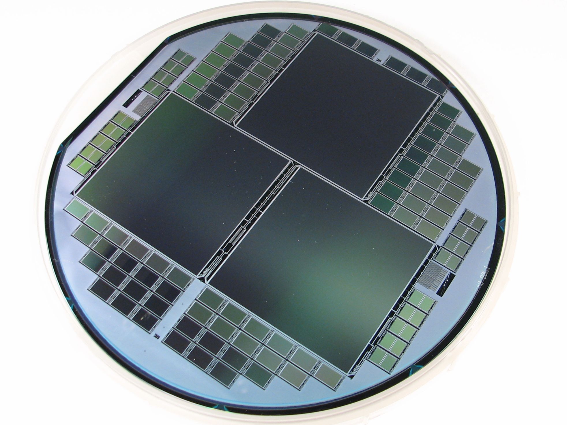
I picked up this interesting wafer at the silicon valley electronics flea market. So far as I can guess, these are some sort of image sensors. The manufacturer has cleverly divided the wafer up to make three different sizes of sensors at the same time– only three of the large ones, and many more in the two smaller sizes.
So, before I pull out the microscope and look for brand names, can anyone guess (or identify) *exactly* what we’re looking at here? For scale, the wafer is about six inches across. A few more pictures follow.
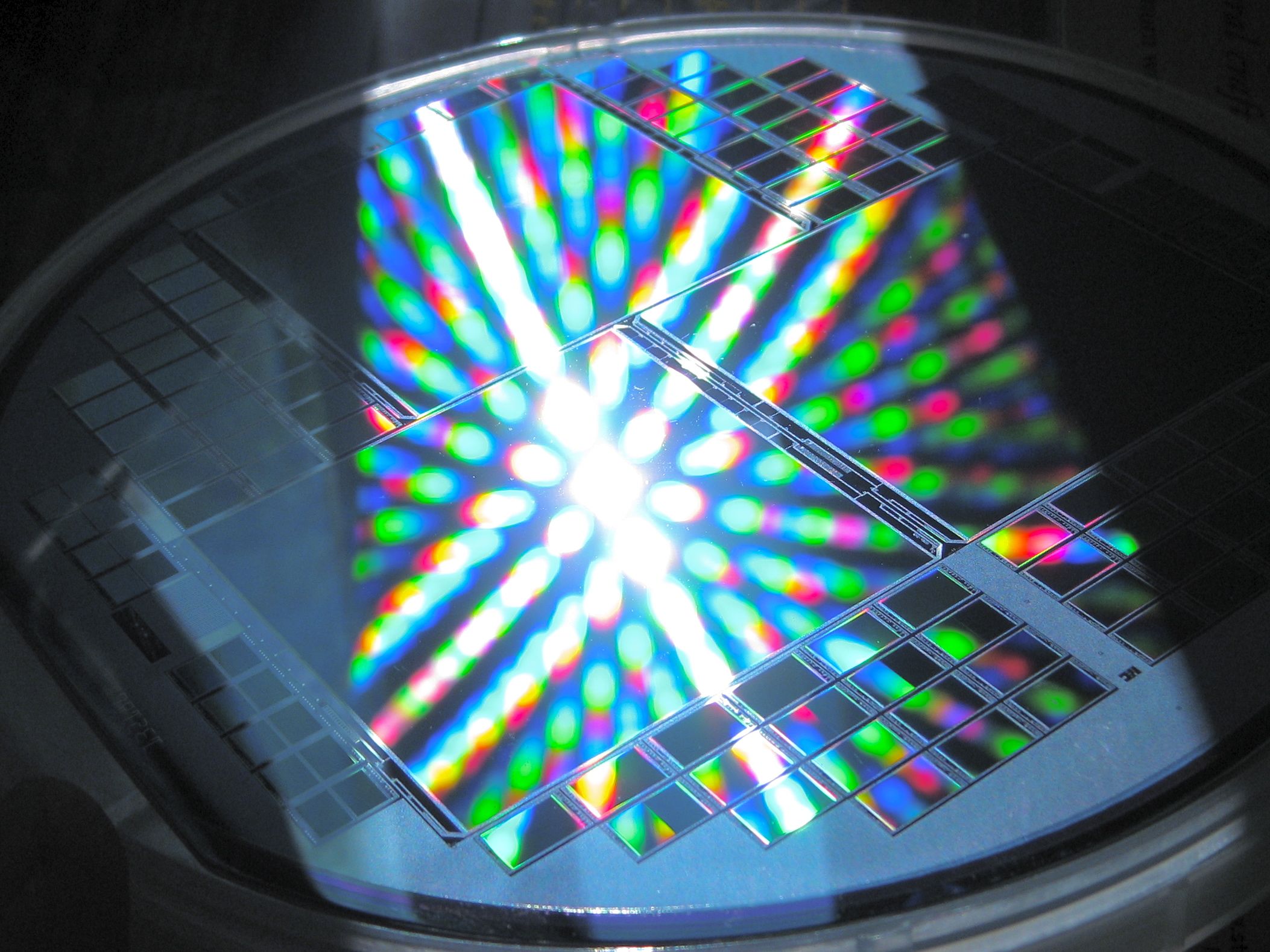
This photo was taken in direct sunlight. The diffraction pattern shows that all of the devices have a high-density microscopic structure that’s basically an equally spaced square grid– obviously consistent with image sensors. And it looks neat.
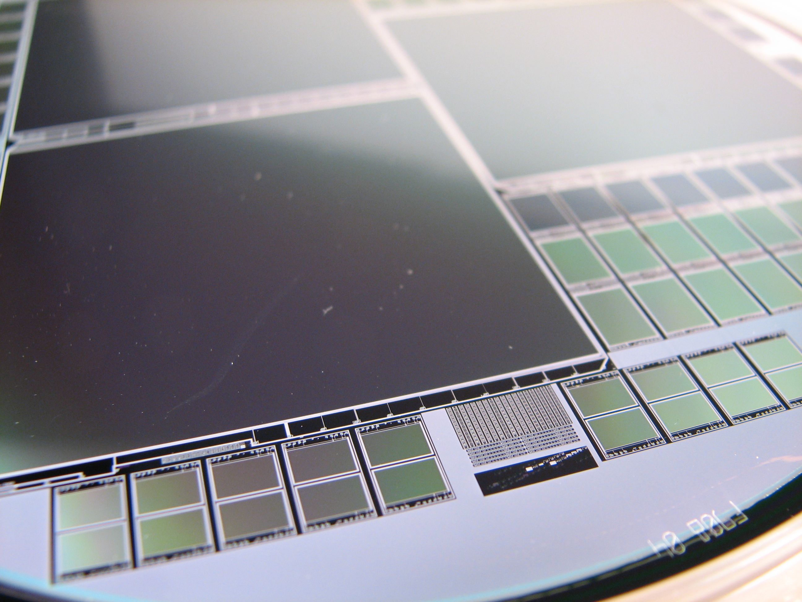
Here’s a second view up close– you can see the different sized devices and a test pattern area. The pictures link to flickr, where full-size images are available.
Update: I’ve found the following part number on the three large sensors: KAI-4300, which then appears to be a Kodak product, in the KAI line of Interline CCDs.

micromirror array for some sort of gigantic projector?
radar detector or sensor for astronomical use in some wavelength.
I wonder if those 3 main sensors are RGB, making this some kind of photo sensor?
I wonder if those 3 main sensors are RGB, making this some kind of photo sensor?
Either a TI DLP chipset, or a group of DALSA imaging chips
Professional cameras use two formats, One is 6×4.5 mm and the other is 6×7 mm. It’s hard to tell from the photo, but it looks like it could be a sensor for the 6×7 format. Professional cameras use removable film holders or removable digital backs so the film can be changed fast or so the camera can be configured to the users need.
The large sensors are probably full-frame 35mm sensors (36mm x 24mm). There aren’t that many companies that make those: Canon, Sony, Kodak, Dalsa and Fillfactory. I don’t think the last 2 are in the business of small sensors for pocket digicams, most likely it is Sony, possibly Canon.
I shouldn’t post while still asleep, I should have said centimeter not millimeter. Profession cameras use a much larger format than 35 millimeters.
My guess: DLP chip of some sort.
Nice find.
See if you can find any "extras". This site has a great collection of photos of silicon chip showing the extra artwork the designers hid within.
http://micro.magnet.fsu.edu/creatures/index.html
Looks like some form of CCD (probably not CMOS) sensors, more likely scientific senors than photographic. I have seen more than a few of these, the arrangement of a few large sensors with smaller chips taking up the remaining wafer space is not unusual.
Why are they round?
Silicon wafers are ‘grown’ as pilars, which is then chopped to discs. Google it.
Lovely pictures. Assuming the large ones are 35mm chips, which would seem likely, the first image gives a very good visual explanation of why a full-format SLR cameras are so bl00dy expensive. Especially since so many of them are rejected – if a silicon wafer has on average 1 flaw, then if it’s all the tiny sensors 4-6mm sensors found in many digicams you maybe have a 1% loss or less – if it’s got 3 big sensors, you stand a high chance of having a 30% loss.
Yes: the bigger the chip, the more difficult it is to make. And also more expensive. Larger wafers are also more difficult to handle.
(I remember when ‘big wafer’ meant three inches across. But I also remember building LED displays for $200 six-function calculators. By hand. At first, it was about one an hour, with one chip for every segment; nine months later, it was 10 an hour, with each digit on a chip of its own. Progress!)
Given how many CCDs are on the chip I have to guess its the main sensor for a mass spectrometer.
Those large image sensors ARE more than sure Kodac Large format sensors…a smaller version of those is used in the Leica S2…thet camera costs 36 grand….the smaller ones could be also Kodac sensors used in M9, M8.2 etc…measure those smaller sensors…if they are 36mm by 24mm they must be the 18Megapixel full-frame sensors you can find in M9’s