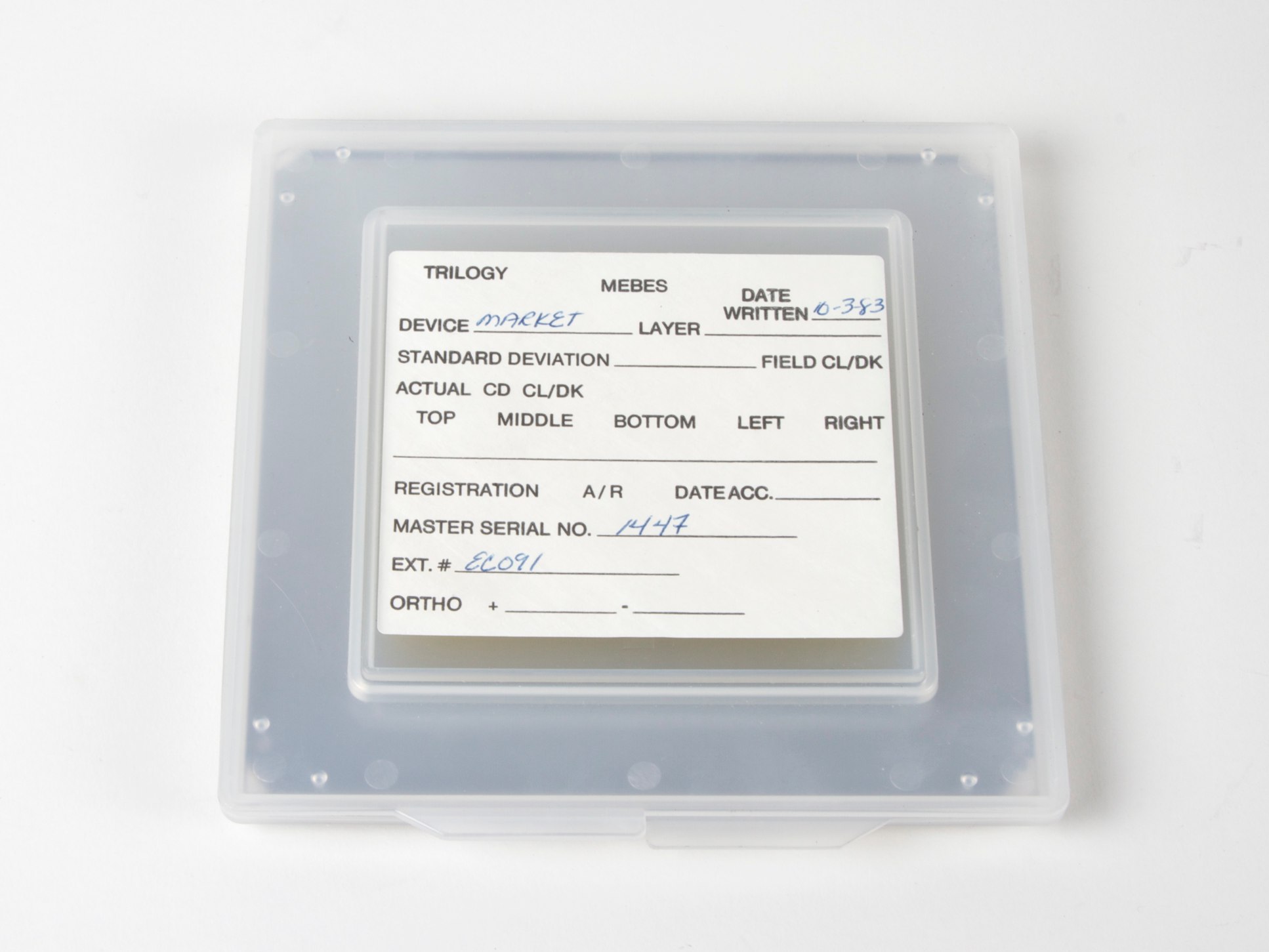
At our local Silicon Valley electronics surplus shops and electronics flea market, we frequently come across all sorts of bizarro semiconductor manufacturing paraphernalia. Here is one of those types that we have written about before, in our coaster project:
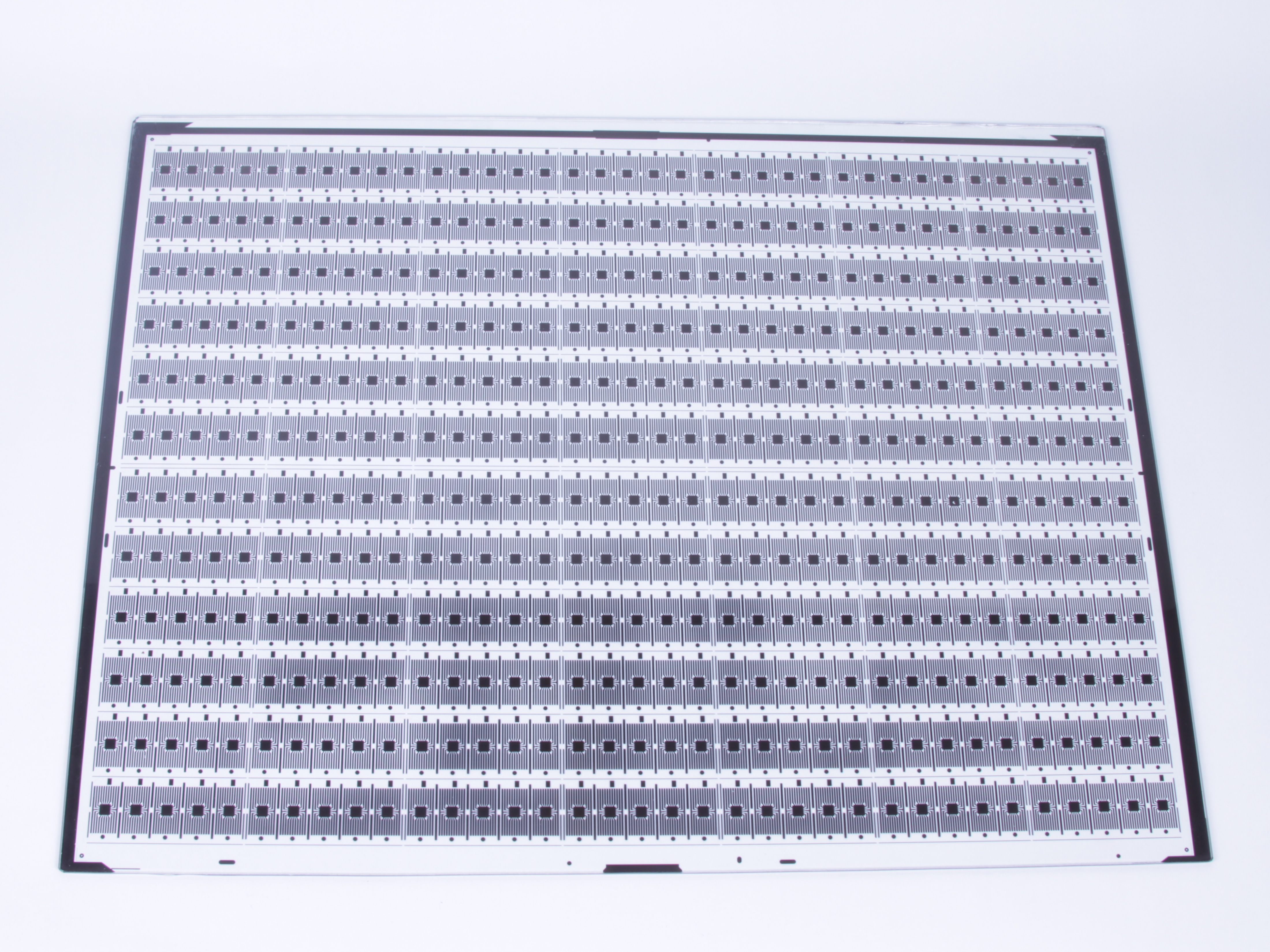
Photolithographic masks, or photomasks are clear templates used in semiconductor manufacturing. Typically, they are made of UV-grade fused silica and have a highly intricate chrome metal film pattern on one side.
The most commonly available masks are test patterns used for calibration, as production masks are guarded carefully. This particular one dates back to 1983!
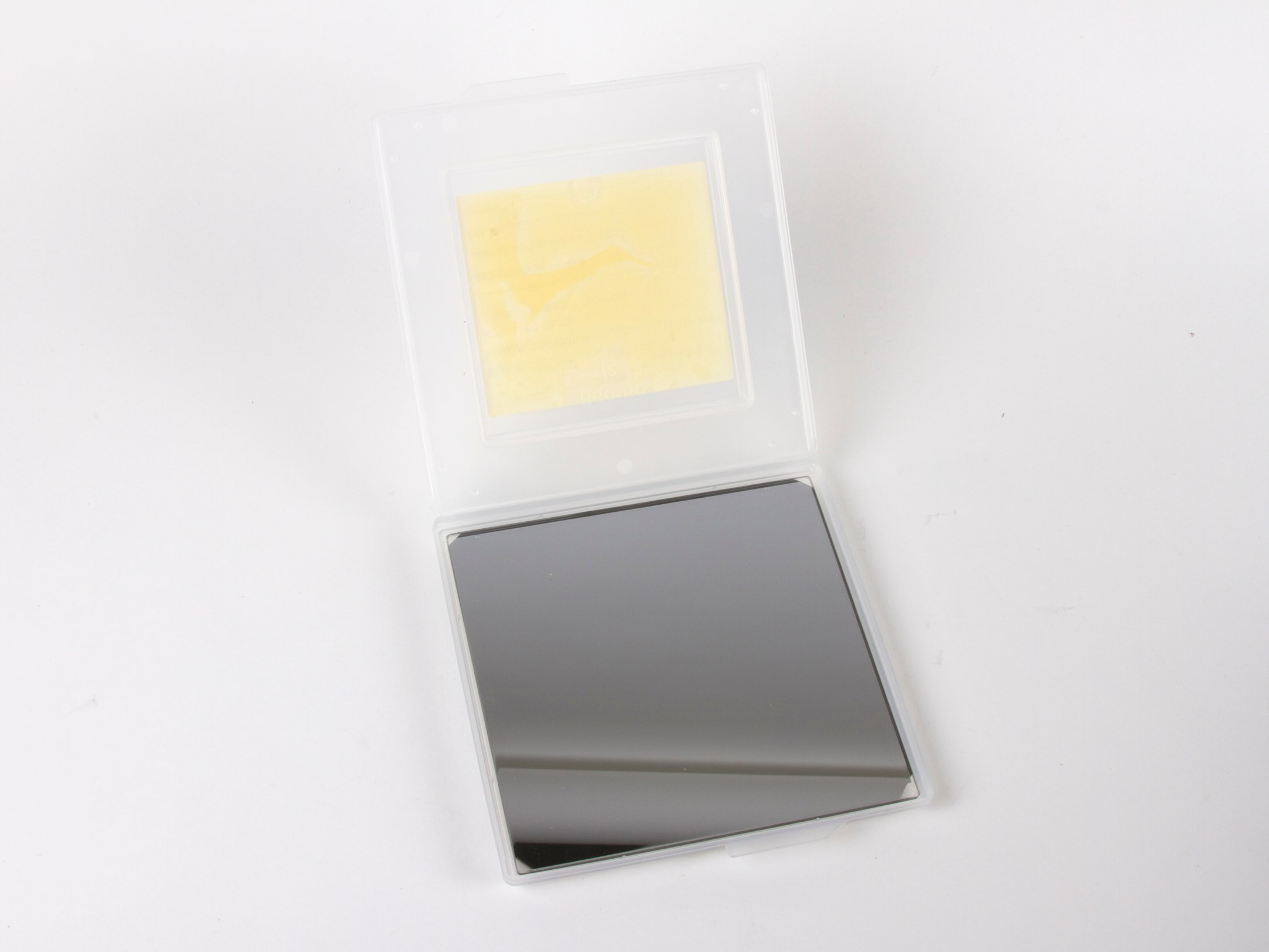
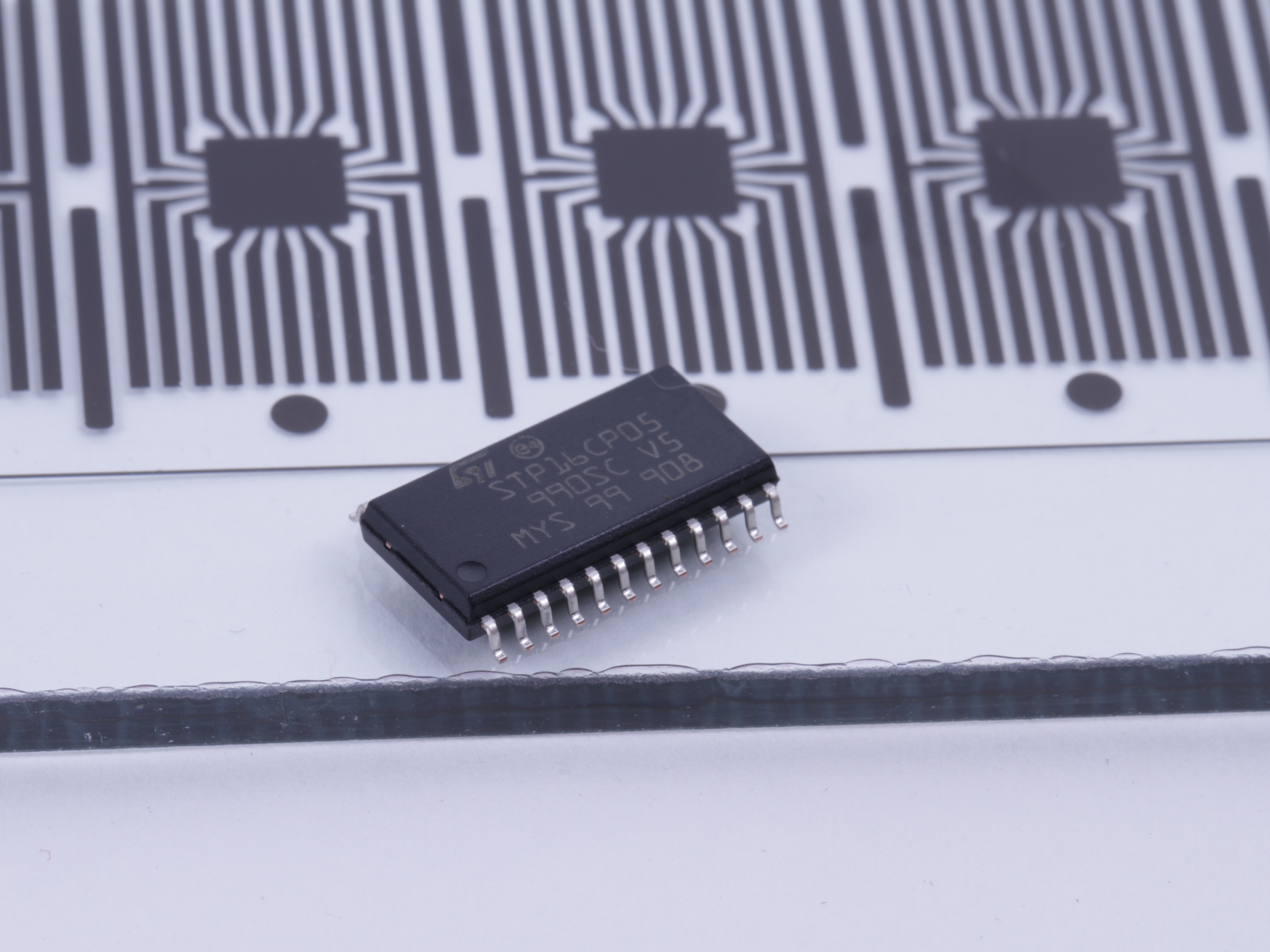
Now looking inside at it, it’s hardly a mask at all. It’s nearly fully silvered—perhaps a mask pulled out before the etching step of its process.
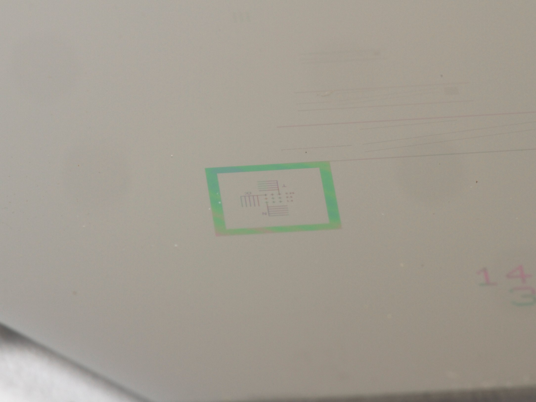
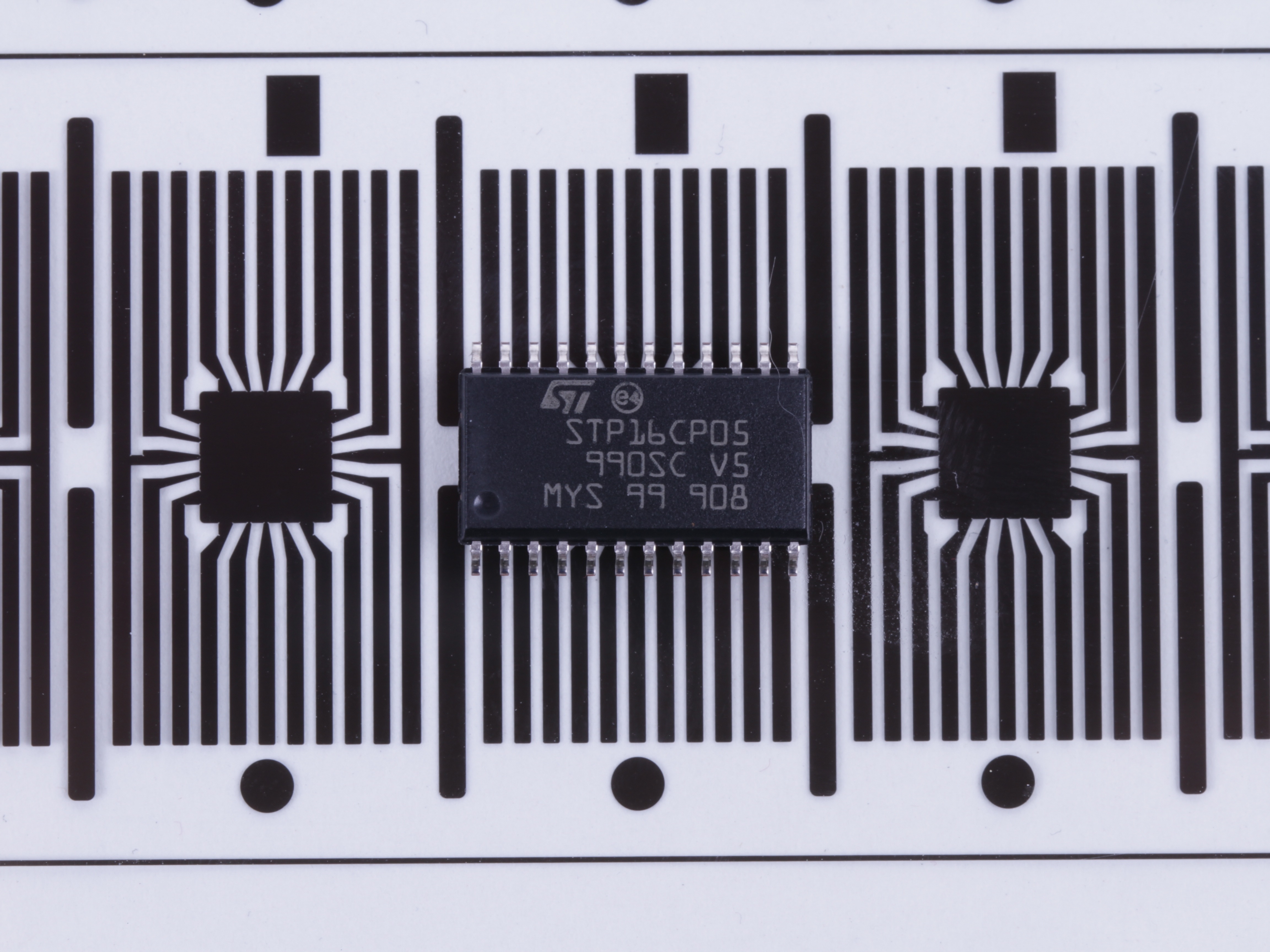
If you look at an oblique angle, you will find a few incredibly detailed patterns, and some printed on markings. This one is marked “5.1 INCH ARRAY” across the top and “1447 3-OCT-83-13. 5” across the bottom.
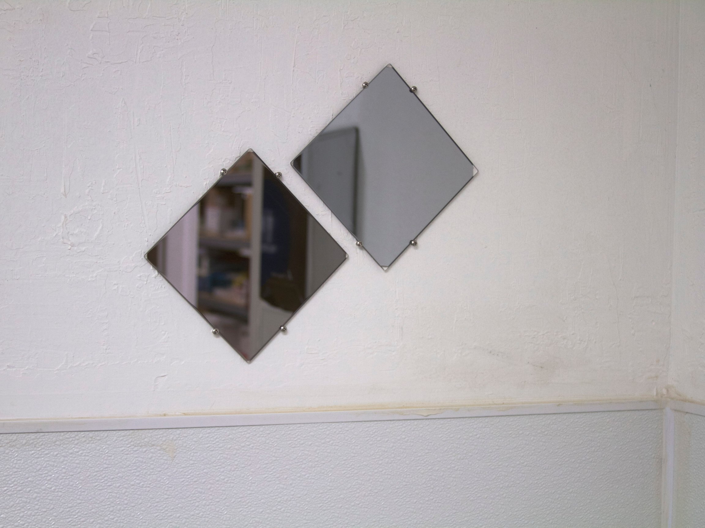
So, what to do with them? Since they don’t have the neat patterns that made those coasters so cool, we used some truss-head screws to mount them to the wall.
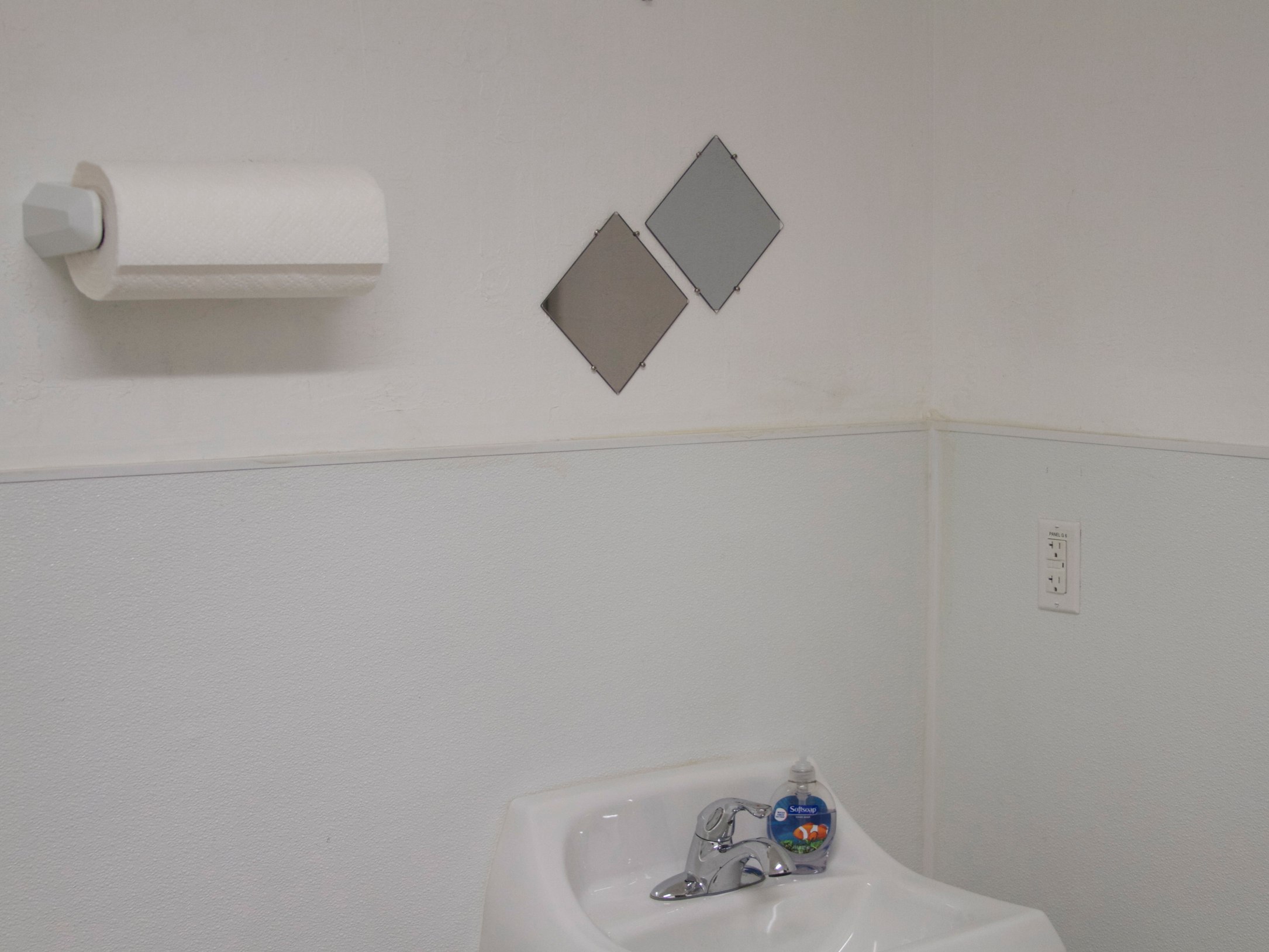
And here we are then, using a couple of photolithographic mask as bathroom mirrors! (With a couple of units at different heights for different-height people.) It solves a couple of problems at once: how to display the beautiful ephemera of semiconductor manufacturing, and what to do about a soulless little extra bathroom at our shop that didn’t come with a mirror.