


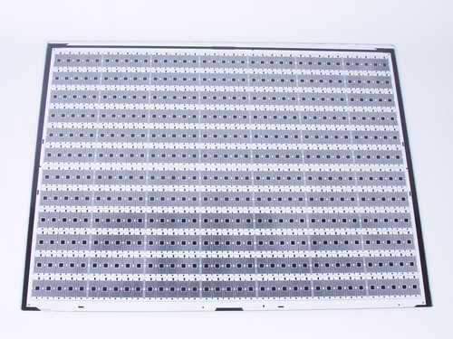
After seeing our photomask coasters, a friend gave us this giant photomask as an art piece. While we’re not certain what this was for, our best guess is that it is a mask for the lead frame for some device in an SO-20 package. The overall size is about 18″ x 24″ and about 1/8″ thick.
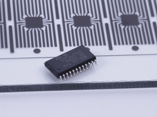
Shown with an SO-24 device on the edge of the plate for comparison. (Didn’t happen to have a correctly sized 20 pin device handy.)

The transparent lines show where the metal will be after processing and the black portions are where the metal will be removed. When you line up the 24 pin device on the plate it is a bit misleading, as it obscures the fact that those two outer transparent lines aren’t actually for device leads. It does confirm that it is sized correctly for a 1:1 mask for a device with a 0.050″ pin spacing, and the central square looks like the right width for a device in an SO-20 package as well.
Tangentially related: CCD wafer

I know this is not a technical article, but your description of the clear being where metal remains on the finished circuit board would create a short for all circuits unless every circuit was cut out as a separate board. A poor design idea I think. ;)
It looks like the device would more likely be a quad style package that has leads on all 4 sides, but it doesn’t have proper lead termination features (pad lands for soldering component leads) and the square in the center would short everything again.
Perhaps it’s for some sort manufacturing process test and not designed for any actual device. I designed circuit layouts for years and this one just doesn’t make much practical sense otherwise.
I don’t follow what you’re saying here; it looks to me like the *black* part would short everything together if it were metal. If the clear part were metal, there’s no shorting, and the lead widths are consistent, and approach a pattern similar to that found in IC packages.
Windell H. Oskay
drwho(at)evilmadscientist.com
http://www.evilmadscientist.com/
And just in case it isn’t clear, this mask makes the lead frame for 420 individual devices. I would love to see the machine that does the clipping and forming, never mind the parts that put the actual chip on and adds the case.
It does appear to be for square chip with pins on all four sides, except on the corners where the last pin on one side is connected with first pin on adjacent side. Very cool though