


Congratulations to reader VAX-Dude for winning the Name that Ware contest for May 2013, by correctly identifying our mystery ware as a VAX 9000 series High Density Signal Carrier (HDSC).
Which might lead you to ask another perfectly reasonable question: What the heck is a High Density Signal Carrier?
To begin with, we’ll reveal two more close-up pictures that we had been reserving— just in case we had needed to give another hint before the end of the contest.
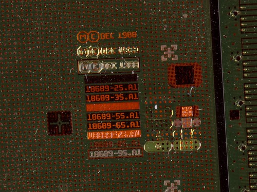
First, a manufacturer and date: DEC (Digital Equipment Corporation), 1988.
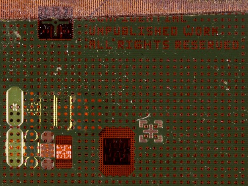
Secondly (and a little harder to read), the text says “CONFIDENTIAL” “UNPUBLISHED WORK” “ALL RIGHTS RESERVED.”

The VAX 9000 was a supercomputer/mainframe computer system released by DEC in 1989. Roughly four dozen of these systems were delivered, starting just under a million dollars each.
In his answer to the contest, VAX-Dude linked to Digital Technical Journal, Volume 2, Number 4, 1990, where there is an article about the HDSC, starting on page 80. This article gives an introduction to the HDSC, its specifications, and its manufacturing process.
To summarize, the performance of mainframe computers in the late 1980s was (in part) limited by the speed of communication between integrated circuits on the circuit boards. One solution to this, which DEC implemented in the VAX 9000 series, was to create tightly integrated Multi-Chip Units (MCUs). An MCU consists mostly of array logic chips (VLSI macrocell array “MCA” chips) and memory chips, connected together through a high-speed interconnect system (the HDSC), mounted together with heat sinks in a field-replaceable housing. Arrays of different MCUs, filling a full shelf of the computer cabinet, would together comprise the CPU of the computer.
Here is what one particular VAX 9000 MCU— a type with eight MCA chips, and one clock generator chip (and no memory chips) —looks like, complete in its housing:

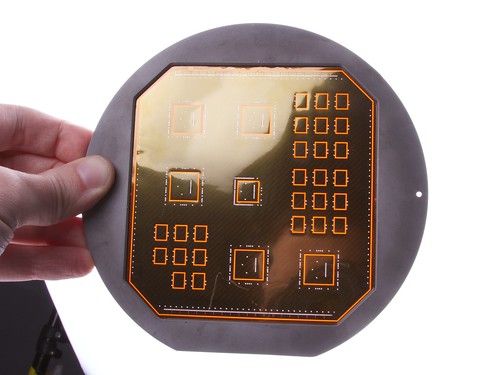
The photos of this MCU come from the blog of Ned Batchelder, who came across this object some time ago, without having seen one before. You may immediately recognize the HDSC substrate, on which the chips are mounted, as being the same basic thing as the central part (that part contained within the stainless frame) of our mystery object.
But, what are all those other things in the photo? Obviously there’s a lot more hardware here than just that substrate.

This exploded view of an MCU, from the VAX 9000 System Introduction, shows the set of parts that you can see in the prior photo. (You may also want to look at a similar diagram on page 84 of the Digital Technical Journal, linked above.)
Comparing this diagram to the photo, note (A) that the exploded view is upside-down from the photo— the signal flex connectors are visible at the top of the MCU, (B) that the HDSC lid is not present, which means that we can see all the way down to the chips mounted on the HDSC, and (C) that the set of chips in any given MCU may vary dramatically from one type of MCU to the next.
There are some important things that you can see in the diagram. First, note giant “signal flex connectors” that wrap over the four sides of the MCU, to carry electrical signals to neighboring MCUs. Then, note the large high-power connectors that are part of the housing, which carry the high current needed to run these power-hungry MCUs.
There is also a copper base plate at the top of the diagram, which sits right below the HDSC in the photograph. The HDSC is a flexible circuit, and it is laminated to this copper base in order to hold it rigid. The chips in the MCU do not actually sit atop of the HDSC, but rather in cut-out holes through it, bonded to the copper plate below, which is in turn connected to the heat sink.
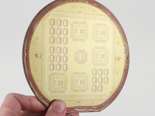
In our original object below, you can see the transparent “cut” lines– where the HDSC will be cut out of the frame, and where the holes for the chips to sit will be cut:
In this close-up of the assembled MCU, you can see that the chips do indeed sit slightly recessed into the HDSC:

The chips (in the black epoxy packages) are mounted in a TAB (metallic gray), a type of two-layer interconnect that fans out from the 100 micron pitch of the IC leads to the 200 micron pitch of the bonding pads on the HDSC.
And that brings us to the HDSC itself. The HDSC is a 8-layer copper and kapton (polyimide) flex circuit designed to provide short, impedance controlled paths for signals going between chips. And it’s made by a rather remarkable process.

Rather than producing them as traditional circuit boards (e.g., starting with thin sheets of kapton and copper), HDSCs were actually manufactured in a semiconductor (“wafer fab”) process. It began with a 6″ semiconductor-wafer shaped piece of aluminum, which was spin-coated with kapton, using the type of machine that normally coats semiconductor wafers with etch resist. The copper layers were added by the same photolithographic techniques used to make metal layers on semiconductor wafers (sputtering and selective etching), but then electroplated to achieve the desired copper thickness. This process was repeated to produce a total of four copper layers. This four-layer “signal core” is laminated to a separately built “power core,” to produce the full sandwich with 8 copper layers.
As part of the process, the circuit is bonded to a steel ring frame and the original aluminum backing wafer is etched away, leaving a stand-alone flex (kapton) circuit, stretched taut across the steel frame like a drum head— just as we found ours —before it is cut out and mounted into the MCU.
Because semiconductor manufacturing processes generally have much, much higher resolution than typical printed circuit board manufacturing processes, the HDSC has remarkably high resolution for a circuit board. The copper traces on these HDSCs were 18 microns wide with 75 micron minimum pitch — equivalent to 0.7 mil trace width and 3 mil pitch. (That is to say, neighboring copper traces can run about as close together as sheets of notebook paper.)
You can read additional technical details about how the HDSCs were manufactured in the book Multichip module technologies and alternatives: the basics, edited by Daryl A. Doane, and Paul D. Franzon. (Preview link for relevant section at Google Books.) A second book reference with great detail is Multichip Modules, edited by Ernest S. Kuh. (Preview link for relevant section at Google Books.) So far as we know, the VAX 9000 was both the first and last time that this particular MCU configuration was used.
Finally, if you’d like to see one more in-frame HDSC like ours, one is apparently on display at Weber State University. Or, if you’d just like to buy a working VAX 9000 MCU to play with, you can occasionally find them for sale on the internet.

Excellent description and pictures. Thanks!
This is a very fine piece of engineering.
Wow, way to make a guy feel old!
I remember having sweaty palms just being around one of these. VAX Clusters, DECNet and let us not forget PathWorks DEC’s answer to Microsoft’s LANMAN oh my…
Let us not forget the AOS/VS vs. VMS wars.
RIP Ken Olsen